Advanced PCB design and layout for EMC Part 4 - Reference planes for 0V and power
This is the fourth in a series of eight articles on good-practice design techniques for electromagnetic compatibility (EMC) for printed circuit board (PCB) design and layout. This series is intended for the designers of any electronic circuits that are to be constructed on PCBs, and of course for the PCB designers themselves. All applications areas are covered, from household appliances; commercial, medical and industrial equipment; through automotive, rail and marine to aerospace and military.
These PCB techniques are helpful when it is desired to…
- Save cost by reducing (or eliminating) enclosure-level shielding
- Reduce time-to-market and compliance costs by reducing the number of design iterations
- Improve the range of co-located wireless datacomms (GSM, DECT, Bluetooth, IEEE 802.11, etc.)
- Use very high-speed devices, or high power digital signal processing (DSP)
- Use the latest integrated circuit (IC) technologies (130nm or 90nm processes, ‘chip scale’ packages, etc.)
The topics to be covered in this series are:
- Saving time and cost overall
- Segregation and interface suppression
- PCB-chassis bonding
- Reference planes for 0V and power
- Decoupling, including buried capacitance technology
- Transmission lines
- Routing and layer stacking, including microvia technology
- A number of miscellaneous final issues
A previous series by the same author in the EMC & Compliance Journal in 1999 “Design Techniques for EMC” [1] included a section on PCB design and layout (“Part 5 – PCB Design and Layout”, October 1999, pages 5 – 17), but only set out to cover the most basic PCB techniques for EMC – the ones that all PCBs should follow no matter how simple their circuits. That series is posted on the web and the web versions have been substantially improved over the intervening years [2]. Other articles and publications by this author (e.g. [3] [4] and Volume 3 of [5]) have also addressed basic PCB techniques for EMC. This series will not repeat the basic design information in these articles – it will build upon it.
Like the above articles, this series will not spend much time analysing why these techniques work, they will focus on describing their practical application and when they are appropriate. But these techniques are well-proven in practice by numerous designers world-wide, and the reasons why they work are understood by academics, so they can be used with confidence. There are few techniques described in this series that are relatively unproven, and this will be mentioned where appropriate.
Table of Contents, for this Part of the series
1 Introduction to Reference Planes
2 Design issues for reference planes
2.1 Plane dimensions
2.2 Dealing with gaps and holes in planes
2.3 Cross-hatching and copper fills
2.4 Connecting devices to planes
2.5 Thermal breaks
2.6 Device placement
2.7 Fills and meshes
2.8 Resonances in the 0V plane
2.9 Cavity resonances in plane pairs
2.10 Reducing the ‘edge-fired’ emissions from plane pairs
2.11 Locating via holes for aggressive signals or power
2.12 When traces change layers
2.13 Component-side planes for DC/DC converters and clocks
3 Splitting a 0V plane is not generally a good idea any more
4 When traces must cross a 0V or power plane split
5 Advantages of ‘High Density Interconnect’ (HDI), ‘build-up’ and ‘microvia’ PCB technologies
6 The totally shielded PCB assembly
7 EMC-competent QA, change control, cost-reduction
8 Compromises
9 References
1 Introduction to Reference Planes
A well-designed 0V reference plane, sometimes called an ‘earth’ or ‘ground’ plane (although it has nothing to do with the safety earth or ground), is increasingly essential as the shrinking feature sizes of ICs decreases the rise and fall times of their logic transitions, as discussed in Part 1 of this series [6]. A well-designed power reference plane might also be required, for the same reason.
The data sheets for digital devices only provide maximum rise and fall times (if they even include that information) – this allows the IC manufacturers to move their devices to smaller fabrication processes. The resulting ‘mask-shrinks’ or ‘die-shrinks’ save them a great deal of money, but can create potentially huge EMC problems for their customers. Some manufacturers have had to spend millions of dollars redesigning existing products to maintain EMC compliance, after their microprocessor manufacturer implemented a die shrink.
Devices such as 74HC ‘glue logic’ series that has been around for nearly 20 years originally used to only emit significantly at up to 200MHz – now the same part numbers from the same manufacturers are found to cause emissions problems up to 900MHz. This makes it important for manufacturers to retest old products that are still in production every few years, to check their EMC compliance. There is no sign of any end to this trend to ever-faster edge rates and ever-higher frequencies, for at least the next 10 to 15 years.
Ideally, a reference plane is a solid copper sheet in (or on) a PCB. It is definitely not a ‘copper fill’ or ‘ground mesh’ (see later).
Unfortunately, copper planes without numerous perforations are impossible in practice without using ‘HDI’ PCB fabrication technology (often called ‘micro-via’, see section 5). This article will discuss how to get the best EMC performance out of PCB reference planes despite the restrictions of typical modern PCB fabrication technologies, such as through-hole-plate (THP) – in which holes are drilled right through a PCB, then plated with metal so as to provide electrical connections between the top, bottom and any internal copper layers.
0V reference planes are the single most cost-effective EMC measure that can be applied at PCB assembly level (or higher). It is hard to understate how important the use of 0V reference planes in PCBs is for EMC. When advanced PCB EMC techniques are required – a well-designed 0V reference plane is absolutely essential.
Planes provide a number of very valuable EMC and Signal Integrity (SI) functions…
- They provide very low impedance, which means they can provide devices and circuits with stable reference voltages at radio frequency (RF).
We normally estimate the impedance of wires or PCB traces to be 1nH for each millimetre of their length, meaning that 10mm of wire or trace has approximately 63#937; of inductive impedance at 1GHz. So when we need to provide a variety of devices with high-frequency currents from a reference voltage (as we increasingly do) we need to use a plane to distribute the reference voltage.
- Their low impedance return path is essential if capacitive filters mounted on the PCB are to achieve good performance above a few MHz. See Part 2 of this series [7] for PCB design for filters.
- They encourage returning RF currents to flow in the path that provides the least emissions and the lowest susceptibility.
When the return RF current path for a signal or power circuit flows in a plane conductor, it can follow whatever path it prefers – and it prefers the path with the least overall impedance. This is the path that achieves the least inductance in the overall current loop (‘loop inductance’), and also the path with highest capacitance to the send path. This concentrates the electric and magnetic fields associated with the differential-mode circuit into smaller volumes; reducing their coupling to other structures and to the electromagnetic environment, thereby reducing their common-mode emissions and improving the circuit’s susceptibility.
- They behave as image planes, so will provide a degree of shielding effectiveness for components and traces that are not close to an edge or a split.
Image planes provide shielding even when they are not connected to the circuit concerned. For example: a trace spaced 1mm above the centre of a large plane, the image plane effect results in at least 30dB of shielding effectiveness at frequencies above 100kHz. Closer spacing of components or traces to the plane gives more shielding effectiveness, so low-profile components are better for EMC.
- They reduce common-mode emissions from the cables attached to the PCB’s circuitry, at the frequencies at which they are ‘RF bonded’ to the plane. This issue was also mentioned in section 2.1 of Part 3 of this series [8].
RF bonding to a plane either means a direct connection, or a capacitive filter, between the conductor and the plane, at the point where the conductor leaves the area covered by the plane. In the case of conductors carrying signals, the value of the capacitor should be low enough not to compromise the signal.
Simply connecting capacitors from an external conductor to a PCB’s reference plane can encourage external noise currents to flow through the plane, and can increase the RF currents from output drivers. These increased RF noise currents flowing in the plane will cause increased noise voltages wherever the plane is imperfect (as they often are, for example where there are clearances around through-hole vias). So these ‘RF bonding’ capacitors will often need to be used with series resistors or soft ferrites on one or both sides to optimise the PCB’s EMC. Refer to Part 2 of this series [7] for the EMC design issues associated with the filtering of signals and power conductors as they enter or exit a PCB.
It is not the purpose of this article to describe the theory of PCB reference planes, but [9], [10] and [11] are very useful references for the issues bulleted above, and cover the relevant mathematics.
2 Design issues for reference planes
2.1 Plane dimensions
As was mentioned above, a reference plane is ideally a solid copper sheet in (or on) a PCB. It is definitely not a ‘copper fill’ or ‘ground mesh’ (see later for using fills and meshes).
Planes must lie under all of their associated components and their traces and the 0V reference plane should extend beyond them on all sides of the PCB by as far as possible. It may even be worthwhile making a PCB larger simply to extend its 0V plane even further beyond the PCB’s devices and traces.
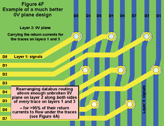
One reason for this is that signal or power return RF currents flowing in the plane layer (or planes) adjacent to the trace follow the path of the trace, but although the highest current density is underneath the trace the RF current also spreads out in the plane to either side of the trace’s route, as shown by Figure 4A.
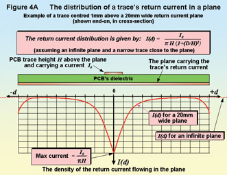
About 95% of the return current is generally assumed to travel in a strip of plane as wide as 3 times the trace-plane spacing (H) or three times as wide as the trace width (W) – whichever is the smaller – centred along the trace’s route. It is considered to be an important basic PCB layout technique not to have any holes, splits or edges in this region of the plane. (Note that the analysis in Figure 4A assumes that H is smaller than W.)
For higher EMC performance, the region of unbroken plane should extend even further away from the route taken by the trace, along both sides of its route. For very high frequency analogue signals or high-rate data with edges of less than 2ns (in real life, not the data sheet specification), it is often recommended that the trace is routed no closer than 10mm from any plane edge or split.
Another reason for extending the 0V reference plane even further is that its RF impedance falls as the plane’s size increases (an infinite plane has zero impedance at d.c.) and most/all of the plane benefits in the bulleted list in section 1 above are improved as a result.
But, like all metal conductors and structures, planes have natural resonant frequencies that depend on their shapes, sizes and environments. So in practice it may be necessary to limit the size of a plane to optimise its overall EMC benefits. Plane resonances are discussed later.
Part 2 of this series [7] described ‘segregation’ techniques in PCB layout. It is important to note that even though segregated circuits will almost always share the same 0V reference plane, the segregation ‘rules’ in [7] still apply in full. (These days it is not generally recommended that 0V planes are split, and this is discussed later.)
Power planes are designed much like 0V planes, but their use is intimately tied up with the power supply decoupling strategy. Decoupling is the subject of Part 5 of this series, and will not be discussed here. It is common for there to be several areas of power plane on a PCB e.g. 5V, 3.3V, 2.8V, +12V, -12V, and when the PCB’s circuits have been carefully segregated it is often possible to fit all of these on a single PCB layer.
2.2 Dealing with gaps and holes in planes
Any gap or hole in a PCB plane is a bad thing for EMC, because it is bound to increase impedance and inhibit the free movement of RF return currents. Where plane gaps or holes (or edges) are far enough away from traces (see 2.1 above) the general EMC guidance for all PCBs is that no gaps or holes should have longest dimensions greater than one-hundredth of the wavelength (λ) at the highest frequency of concern (i.e. the highest frequency to be controlled for EMC).
In air or vacuum, λ = 300 ÷ f (λ in metres gives f in MHz). But if the gap or hole is filled with something other than air or vacuum, the dielectric constant, k, (= relative permittivity) of the filling material will shorten the wavelength according to: λ ÷√k. For example, if the plane gap or hole is filled with PCB substrate (assumed to be FR4 unless stated otherwise), its k of 4.0 at frequencies above 1MHz means that its l is half what it would be in air or vacuum: λ = 150 ÷ f (λ in metres, f in MHz).
Modern PCBs have such high densities that through hole plate (THP) PCB manufacturing techniques cause massive perforation of any planes, due to the clearance holes (antipads) required around each via. Such high levels of plane perforation cause a significant increase in plane impedance and reduce all of the benefits bulleted in section 1 above.
To improve EMC, antipads should be as small as possible – but without causing significantly decreased yield in their manufacture. However, some manufacturers use very low-cost PCB manufacturers whose accuracy in aligning PCB layers is very poor compared with what is typically achieved these days, and so require very large antipads to keep costs down. In such cases it will often be more cost-effective overall to use a better PCB manufacturer, and shrink the antipad diameters to 1mm.
There are specialist manufacturers who can provide much smaller antipads diameters than 1mm, at a price. But plane perforation by antipads can be largely eliminated by the use of HDI PCB fabrication technology (see section 5) that gives the best EMC performance from the planes.
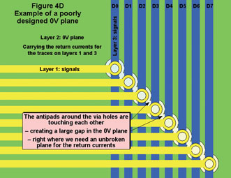
Another important issue with dense THP PCB layouts is that the antipads should not merge into each other to create larger gaps or slots in a plane. This often happens when via holes are placed too close together; and/or when the computer-aided-drawing (CAD) system is set up to have too large a minimum radius when drawing planes; and/or when a PCB manufacturer overexposes the plane layer phototools. Figure 4B gives some examples of antipad merging errors.

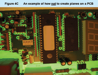
Figure 4C shows an example of how not to create planes on a PCB. This PCB could have had acceptable EMC performance using microprocessors purchased in the 1980s, but not with those purchased this millennium (even if they had the same type numbers).
Via holes that are placed too close together can easily be detected by a review of the draft layout, and then corrected. CAD plane drawing rules are often set to a large minimum radius to shorten processing time to help speed design – which is acceptable as long as the final checking plots are created with a small minimum radius to prevent antipads from merging.
PCB fabricators who overexpose plane layer phototools to avoid having to take care over layer registration should never be used again, as their corporate quality culture is obviously deficient. Often, early deliveries of a PCB design use the antipads diameters that were designed, but when the product has settled down in regular production some suppliers will ‘grow’ their antipads to improve their yields. So it is always worthwhile carrying out simple checks on deliveries of bare PCBs, including a check on antipads diameters.
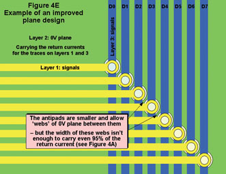
When a PCB has a large number of through-holes and via holes, care should be taken to prevent their antipads from merging together or encroaching on the current return paths of the traces (see Figure 4A). Figures 4D, 4E and 4F show how careful design can overcome these problems.
Most PCB designers would be able to improve on the layout of Figure 4F, but at least it illustrates the point.
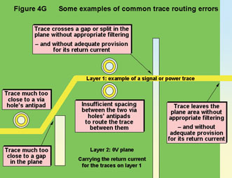
Figure 4G shows some of the common mistakes when traces are routed too close to antipads, plane splits or edges, thereby adding impedance to the return currents associated with the traces and worsening EMC. Note that from a SI viewpoint, adding impedance in a return current path has the same bad effect on waveshape as adding impedance in the send path (i.e. in the signal’s trace).
Planes are made of the same thin copper foil that is used for signal traces, so their resistance can sometimes be a problem where heavy d.c. or low frequency currents are employed. PCB manufacturers can ‘plate up’ the standard ‘½ounce’ (½oz) or ‘1oz’ foil thickness up to 8oz, to reduce plane resistance. Some PCB manufacturers can laminate metal sheets into a PCB, for use as a heat sink (sometimes called ‘thermal clad’ PCBs). Where their process allows the plated through holes and vias to make a reliable electrical connection to the metal sheet, plane resistance can be reduced considerably. Bonding the PCB’s 0V plane to its chassis can also help reduce plane resistance, and techniques for doing this were described in [8].
2.3 Cross-hatching and copper fills
A copper fill is not a plane, it is just a mess of RF resonators and antennas and worsens a PCB’s EMC performance. If there is an unbroken copper 0V reference plane layer on a PCB, a copper fill on another layer can be prevented from behaving as a mess of RF resonators and antennas by linking all parts of the fill to the unbroken 0V plane with via holes at least every λ/10 (λ/20 or less would be even better) at the highest frequency of concern, taking the k of the PCB’s dielectric into account (nominally 4.0 for FR4). For example, to prevent copper fills from acting as antennas at up to 1GHz, they should be via’d to the unbroken 0V reference plane every 15mm along their length and over their areas (preferably every 7.5mm or less).
A question that arises sometimes is whether a plane area should be created as a cross-hatched grid, rather than a solid copper area. Cross-hatched plane areas were used to help avoid PCB warping during automated soldering (where the whole PCB is heated) due to unequal amounts of copper on different layers (sometimes called ‘copper-balancing’). Cross-hatched plane areas were common in the 1970s when the slow silicon technologies typically used in ICs allowed us to use double-sided PCBs with only partial plane areas.
But a cross-hatched plane, even if extended to the full size of a PCB instead of being shared with traces, gives nothing like the EMC benefits of a solid copper plane. So to achieve copper balancing when using solid copper planes we must pay attention to the stack-up of the PCB, to balance the plane layers to achieve a symmetrical construction. (Stack-up will be one of the issues discussed in Part 7 of this series.)
Copper balancing using plane layers can sometimes result in more layers than are thought necessary for SI or EMC. In this case it is sometimes possible to add copper fills to one or more trace layers to prevent board warping during automated soldering. But remember that all parts of the copper fills must be via’d to an unbroken 0V reference plane at least every λ/10 at the highest frequency of concern, so they don’t worsen EMC.
2.4 Connecting devices to planes
Having gone to the trouble of creating planes with very low impedances (over the frequency ranges where we want to control EMC) – the benefits of the planes can be compromised by the impedance of the connections between the devices and the planes. So we need to minimise the inductance of the component-to-plane connections. This generally means (in order of importance)…
- Reducing the length of any trace (‘via-in-pad’ is best)
This applies to any trace used to connect the component’s solder pad to the through/via hole that connects it to the plane layer.
- Increasing the width of any trace (applies as above).
As a general guide, the inductance per millimetre length reduces as the square root of the increase in trace width. So halving the inductance requires the width to be increased four-fold.
- Reducing the spacing between the plane and the component, in the PCB’s ‘stack up’.
This will shorten the length of the through-hole or via hole that is carrying the current, reducing its inductance. It is usually assumed that plated holes add a ‘partial inductance’ of about 1nH for each millimetre of their length that carries current (25nH/inch).
- Where through-holes or via holes carry opposing currents (e.g. the 0V and power pins of an IC) – placing them very close together (e.g. 1mm, or less if practical)
Close spacing of opposing current paths maximises the mutual inductance between the two holes, effectively ‘’cancelling out’ a proportion of their partial inductance. For example: two 0.5mm diameter via holes each carrying opposing currents for 1mm of their length, add a total of 1.2nH (0.6nH each) if they are 5mm apart, but only 0.53nH (0.26nH each) if they are spaced 1mm apart.
- Using multiple through-holes or via holes in parallel. The reduction in inductance is greater, the further they are apart. But if traces have to be used to increase the spacing, their extra inductance will reduce the benefit of paralleling.
- Increasing the diameter of a plated hole to decrease its partial inductance. As a general guide, the inductance per millimetre length reduces as the square root of the increase in diameter. So (for example) halving the inductance requires the diameter to be increased four-fold. Significant reductions in inductance therefore require quite large holes, with correspondingly large antipads perforating the planes, which can reduce the EMC benefits from those planes.
Figure 4H shows how these requirements are applied to the layout of some example decoupling capacitors.
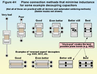
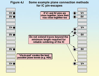
Figure 4J shows how the bulleted requirements above are applied to some examples of component pin-escapes that connect to planes.
‘Via-in-pad’ has been mentioned above, and means that the plated hole that connects the component pad to the plane does so directly – the hole is situated within the pad’s area. Holes that penetrate right through a PCB, as is normal with THP PCBs, can ‘steal’ solder from the component’s terminal, possibly leading to dry joints and unreliable circuit operation with some kinds of automated soldering processes.
It is generally considered that via-in-pad can be used with THP PCBs that are wave-soldered, but that it is not a suitable technique for reflow soldering. However, the author knows at least one electronic manufacturer in the UK that uses via-in-pad on reflow soldered THP boards without any apparent yield or reliability problems. So it seems that some PCB manufacturers have skills or processes that others may not, and it may be possible to take advantage of their abilities to improve EMC cost-effectively.
Via-in-pad is normal practice when using HDI PCB technology (see section 5), because the via holes are very narrow in diameter and ‘blind’ – they end in a metal wall and do not go right through the PCB, so they steal very little solder. This is one of the reasons why HDI or microvia PCBs are so good for EMC.
2.5 Thermal breaks
Planes were first used on PCBs for leaded components, and the thermal inertia of the plane often made the leads that connected to it harder to solder automatically. So it became commonplace to use a “thermal break pad” on the plated through-holes that connected to a plane. Thermal break pads use a thin trace (or traces) to connect the barrel of the through-hole to the plane, on the plane’s layer, thereby reducing the amount of heat lost to the plane during soldering and making the automated soldering of PCBs using planes easier.
As a result, many PCB designers got into the habit of always using thermal break pads on any plane connections, and this was made a rule in some PCB design departments. Thermal break pads increase the impedance of the plane connection, and whilst this was not significant for a leaded component (since there was a much higher impedance in its leads anyway) it can be important when using surface mounted components. These days, the impedance of a thermal break can be enough to reduce EMC performance at the high frequencies that are of concern these days.
For improved EMC without compromising automated soldering, thermal break pads should only be used for the through-holes associated with leaded components. They should not be generally used for via holes or the plane connections of surface-mounted components although they may be needed for ‘via-in-pad’ designs. Where thermal break pads seem to be necessary, they should be carefully assessed to see if they could compromise EMC. Maybe an adjustment to the normal automated soldering process might be enough to avoid the need for thermal breaks.
2.6 Device placement
The electrical activity in ICs and other semiconductors creates intense local fields around them. Where these fields couple with conductors, common-mode (CM) currents will be created. To optimise EMC these ‘leaked’ CM currents need to be returned to the silicon junctions they originated from as quickly as possible. Luckily, planes make excellent return paths for CM currents.
So, just as for traces (see above and Figure 4F): ICs, other semiconductors and crystals, should never be placed near plane edges, splits, or gaps. For high speed devices – e.g. ICs carrying digital signals with actual rise or fall times of under 2ns (real rise/fall times, not data sheet specifications) or analogue signals with frequencies of more than 200MHz – an unbroken plane is usually required under the IC and extending at least 5mm beyond its periphery.
A top or bottom 0V plane under an IC helps improve its EMC by providing an ‘image plane’ which is closer to it than internal plane layers can be. So, even when overall planes aren’t used on outer layers (see below), small plane areas under noisy devices (e.g. clock generators or buffers) can help, but they must always have multiple vias, spread over their whole areas, to an unbroken internal 0V plane.
Usually, a larger area of unbroken plane around an IC means better EMC: 10 or 15mm is not an unusual requirement even for 8-bit processors running at 16MHz on four-layer boards. Higher-speed devices need more attention to the design of their local planes. Unfortunately, the areas of the planes closest to an IC are usually the most highly perforated of any areas of the PCB, due to the antipads associated with the via holes for all the pin escapes.
Antipad diameters can only be reduced so far using ‘traditional’ THP PCB fabrication, but device pin-count is increasing so plane perforation near ICs is increasing. This problem is another reason for seriously considering the use of HDI PCB technology (see section 5).
The PCB’s stack-up is also important, with closer proximity of an IC to its nearest plane layer helping to improve EMC. Stack up issues will be considered in Part 7 of this series.
2.7 Fills and meshes
There is often great pressure from managers to reduce the number of layers on a PCB, to minimise the cost of the bare board. But the profitable selling price of a product has no direct relationship with the cost of its Bill Of Materials (BOM) – despite what many engineers and their managers still seem to persist in believing. This issue was discussed in detail in Part 1 of this series [6].
Nevertheless, it helps profitability if the cost of a bare board can be reduced by reducing the number of layers – but only as long as this does not create problems for SI or EMC that delay market introduction, require additional costs for filtering and shielding, or create unreliable or non-compliant products. So PCB layer reduction should now only be implemented as part of overall product EMC (emissions and immunity) and SI schemes under the control of competent staff supported by the necessary tools.
Another point to understand is that in reasonable volumes, 4 layer PCBs now cost little more than 2 layer (typically 20% more). But most PCB suppliers specialise in PCBs with a certain number of layers, usually 1, 2, 4, then 6 or more. So (for example) the PCB manufacturer that gives the best price for a 2-layer board will generally not give the best price for a 4 layer. Many engineers in companies using PCBs with 4 layers or less are put off increasing the number of layers, because their buying departments simply ask their usual suppliers for a price and don’t ‘shop around’ as they should.
Planes are the single most powerful and cost-effective EMC technique available in PCB design. So trying to save costs by reducing the numbers of plane layers often results in increased costs overall, plus delay in time-to-market, and maybe increased warranty costs too (due to increased unreliability in real life electromagnetic environments).
When using 2 layer THP PCBs it is best for EMC to try to get all of the traces on one layer (usually the component side), and make the second layer as solid a 0V plane as possible. Where trace crossovers are required, it is best to use wire-link crossover components (‘zero-ohm links’) instead of ‘sneaking’ traces into the 0V plane area. If traces must be ‘sneaked’ into the 0V plane, they should be kept as short as possible. This technique is easiest to apply on analogue circuits, and the author has used it to improve the immunity of a domestic/commercial passive infra-red security device in an unshielded plastic housing, from 5V/m at 900MHz, to 50V/m, making false alarms due to nearby cellphone use very much less common.
Where it is impractical to employ an unbroken 0V reference plane in a PCB, a 0V mesh (or grid) should be created instead. A mesh should, usually achieve some useful degree of control over SI and EMC at frequencies up to those with a wavelength (in the PCB dielectric) no less than 10 times longer than the longest mesh dimension (its diameter or longest diagonal, D). In other words, for FR4 PCB dielectric with a k of 4.0: f<MAX = 15/D (D in metres gives fMAX in MHz).
So, for example, an FR4 PCB with a 0V mesh with a D of 20mm should give some useful control up to 75MHz, with progressively less benefit up to maybe 250MHz. Above 250MHz it will give complex behaviour, probably including amplification of emissions and worsening of susceptibility at some frequencies. Remember that ‘some useful control’ does not mean the kind of performance that would be achieved by an unbroken copper sheet of the same area.
To achieve a meshed 0V area (it cannot be called a plane) on a 2-layer THP PCB, it is usual to route the two layers perpendicular to each other, then do a ‘0V copper fill’ on both layers. Next, the top and bottom copper fills are ‘stitched’ together with manually placed via holes to make a mesh. This usually results in some large areas where there is no mesh – usually close to the microprocessor because the trace density is usually highest in that area.
Unfortunately, for the best EMC from our PCB we need the best control of the highest frequencies closest to the microprocessor, so it is normal to have to spend some time iterating the layout and redoing the copper fills and stitching, to improve the quality of the mesh (reduce the size of D for each mesh element) over the whole PCB and especially near any microprocessors and their crystals and support ICs.
2.8 Resonances in the 0V plane
All conductors have electrical resonant frequencies that depend on the impedances of the media around their edges, just as they have acoustic resonant frequencies. A long thin conductor (e.g. a wire or trace) can be terminated in its characteristic impedance to its return conductor at one or both of its ends, to prevent any resonances – but this option is not available to 0V planes.
The resonant frequencies of a rectangular plane are given by:
fRES = 150 × √{(l/L)2 + (m/W)2}
This formula gives fRES in MHz if L and W (the plane’s length and width) are in metres. l and m are integers (0, 1, 2, 3 etc.) and correspond to the various modes of resonance, but it is usually only the first (lowest) resonant frequency we are most concerned with and this is easily found from: f = 150/D, where D is the plane’s longest diagonal dimension (D in metres gives the frequency f in MHz, D in millimetres gives it in GHz).
At its resonant frequencies a 0V plane can behave as a significant antenna, causing increases in emissions and worsening immunity. This appears mostly to be a problem for sensitive analogue circuits exposed to high levels of RF fields, for example during testing for immunity to automotive industry immunity requirements. However, the segregation techniques described in [7] and the decoupling techniques described in Part 5 of this series – plus the circuit design techniques described in [1] to [5] – will help to reduce the effect of 0V plane resonances.
Where resonances in the 0V plane cause problems, it may be necessary to split the plane to create smaller plane areas for the problem circuits – but how the signals and power cross the resulting plane gap(s) is crucial and can easily cause emissions and immunity problems that are much greater than the improvements achieved by splitting the plane. Crossing plane gaps with low-frequency analogue signals is not difficult, using the techniques described in section 3 below using RC or LC low-pass filters (where the L is a soft ferrite bead) designed to give good attenuation up to the highest frequency of concern [12], [13]. However, crossing plane gaps with high frequency or high speed signals is very difficult.
In the 1980’s, splitting 0V planes used to be considered good EMC practice. But the short rise/fall times achieved in real life by modern ICs now makes splits a major embarrassment for EMC. Plane splits are such a big problem for EMC that for many PCBs it is much better to use an unbroken 0V reference plane over its whole area. The issue of splitting planes is very important, especially given its history as a recommended EMC technique, so it is discussed in detail in section 3 below.
2.9 Cavity resonances in plane pairs
Two or more 0V planes are employed in a PCB to permit the use of transmission-line traces on several layers (see Part 6 of this series); or to route stripline transmission lines; or for ‘copper balancing’ (see above) to prevent board warp during automated soldering. 0V and power planes are often used as adjacent pairs in PCB stack-ups, to provide high-frequency decoupling of the power supplies to the ICs (see Part 5 of this series).
But pairs of planes can suffer from cavity resonances in exactly the same way as was described in Part 3 of this series [8], for the cavity resonances between a 0V plane and a metal chassis. And when they resonate their impedances at some locations can be much higher than normal, and their voltage differences at those locations will be much higher too.
The natural resonant frequencies for a rectangular plane pair are given by similar equations as were used for a single rectangular plane, above, and for a rectangular plane-chassis [8] cavity. But because the cavity between the planes is now filled with a PCB substrate with dielectric constant k, the speed of electromagnetic propagation in the cavity is less and this makes the frequency associated with a given wavelength lower. So the resonant frequencies of a plane pair filled with k are given by: fRES = (150/√k) × √{(l/L)2 + (m/W)2}
This formula gives fRES in MHz if L and W (the plane pairs ’s length and width) are in metres. l and m are integers (0, 1, 2, 3 etc.) and correspond to the various modes of resonance, but it is usually only the first (lowest) resonant frequency we are most concerned with. For FR4 material (k nominally 4.0) this is easily found from: f = 75/D, where D is the plane’s longest diagonal dimension (D in metres gives the frequency f in MHz, D in millimetres gives it in GHz).
For non-rectangular planes that are not simple shapes, it will usually be easiest to determine their resonant frequencies by computer simulation using field solvers, or measurement of a test PCB. But their lowest resonant frequency will still be easily estimated as 75/D MHz (for FR4, with k = 4.0) where D is the plane’s longest dimension, in metres.
To prevent cavity resonances from occurring in the frequency range of concern for EMC, all the 0V planes (including any small or broken plane areas) should be interconnected with via holes spaced no more than λ/10 at the highest frequency of concern, taking the dielectric constant of the PCB, k, into account as described above. So, for example, to prevent cavity resonances in a plane pair at frequencies up to 1GHz, plane-linking vias should be located no more than 15mm from each other, all over the planes’ areas. Closer spacing of the vias will give better EMC.
Figure 4K shows a tested example of a small test PCB with its top and bottom layers dedicated to unbroken 0V planes. This was not a functional PCB, just something to test the idea of linking 0V planes together with vias to see the effect on the cavity resonant frequencies. Figure 4K shows that the first resonance at approximately 2GHz was moved higher in frequency by the addition of some interplane vias, giving a 20dB reduction in plane impedance at 1.5GHz, implying a significant improvement in EMC performance up to that frequency.

The partial inductance of the via holes (at 1nH per mm of their length) prevents them from being a perfect short-circuit between 0V planes, especially at the very high frequencies (1GHz and above) that must be considered in modern PCBs. For example, a 1.5mm via hole has an impedance of about 10Ω at 1GHz.This should be compared with the natural impedance of a solid 0V plane at 1GHz, which can be lower than 0.03Ω if it is far from resonance, and as much as 10Ω at its resonant peak.
0V/power plane pairs obviously cannot be stitched together with vias, instead, we use ‘decoupling’ capacitors, often known as ‘decaps’. Unfortunately, discrete decaps are severely limited in their effect above 500MHz due to their internal self-inductance and the inductance of their current loop comprising pads, traces, via holes connecting them to the 0V and power planes, and the area they enclose.
However, we can place 0V and power planes much closer together in the PCB’s stack-up, and this reduces the fringing fields around their edges – the principal cause of emissions from a plane pair. Halving the 0V/power plane spacing generally halves the emissions – if all else is held equal – but reducing the spacing between 0V and power plane can also reduce emissions (and improve immunity) for a given circuit, as discussed in Part 5 of this series. The fringing fields around a pair of planes are sometimes called ‘edge-fired’ emissions.
One of the consequences of very close 0V/power plane pair spacing – 0.05mm (2 thou) or less – is that the peak amplitude of their impedance at resonance is decreased. Another way to put it would be that the ‘Quality factor’ (Q) of the cavity is reduced. By using much thinner dielectric layers than normally used in THP PCBs it is possible to reduce the Q to 1, at which point the cavity created by the planes does not resonate at all, no matter what its size or shape. This will be discussed in more detail in Part 5 of this series.
One of the reasons for the high Q of the cavity formed by a pair of planes (where their spacing is more than 0.05mm) is that there is very little loss in the cavity to provide damping. In fact, real PCBs usually have lower peak resonances than suggested by simple computations or test boards, because of the damping provided by the presence of lossy electronic components. Damping can be deliberately added by replacing some of the interplane vias by resistors with between 2 and 10Ω. In the case of 0V/power plane pairs, some of the decaps have a resistor added in series with them. Some component manufacturers are understood to have standard products consisting of a capacitor in series with a resistor, specifically for 0V/power plane pair damping.
There usually only need be a few damping resistors spread around a PCB, for best effect they should be placed at the resonant ‘hot-spots’, where the RF voltage differences between the planes are the highest. For simple plane shapes it is possible to predict where the lowest frequency resonant ‘hot spots’ will probably occur, although device loading may modify their actual locations. Computer simulation or experiments will probably be required on most PCBs to find the best locations.
Loading the PCB’s dielectric with particles of ferrite absorber also helps dampen resonant peaks, and may well reduce emissions in other ways. But this is not yet a common method, because the ferrite particles increase the wear on the PCB punching and drilling tools. Maybe when laser-drilled HDI PCB technology (see later) becomes commonplace, ferrite-loaded substrates will become more attractive.
Another way to reduce cavity resonances is by careful design of the planes’ shapes. This will have little effect on the lowest frequency, which is governed simply by the longest dimension, but may have a useful effect on some of the higher frequency resonances.
Where the length (L) of a rectangular plane is an integer or other simple multiple of its width (W), such as 1, 1.5 or 2, the resonant frequencies of the length and width directions will coincide at some frequencies, causing higher-Q peaks (more intense resonances) than usual. Murphy’s law tells us that when the clock frequency is changed just before product launch to get the best performance out of the latest microprocessors, these higher than usual resonances will just happen to coincide with an important clock harmonic that cannot be filtered out, causing problems for EMC compliance at a time when it is very costly and time-consuming to make any changes and delay that cannot be tolerated.
So it is best to avoid square planes and simple L:W ratios – ideally, choose irrational numbers. There is an infinite number of irrational numbers to choose from and the author recommends the use of the ‘Golden Mean’: 1.618…etc… (call it 1.62), because (as Renaissance artists and ancient Greek architects knew) – it gives a pleasing appearance. Thin planes should always be avoided (i.e. the L:W ratio should never be larger than 3 or smaller than 0.33). It may also help a little to have non-parallel plane edges, and to avoid simple regular shapes such as rectangles or circles.
2.10 Reducing the ‘edge-fired’ emissions from plane pairs
When plane pairs resonate, their emissions come from the fringing fields at their edges. This is why they are sometimes called ‘edge-fired’ emissions. 0V/power plane pairs can reduce their edge-fired emissions by reducing their spacing, as described earlier, but this technique cannot generally be used for multiple planes.
We would like to have some way of reducing these edge-fired emissions that did not involve costly enclosure shielding, and one technique that is sometimes recommended is the ‘20H rule’. The 20H rule requires all reference planes (0V or power), except for the main 0V reference plane, to be smaller than the main 0V plane by 20 times their layer spacing. This modifies the shape of the fringing fields, but there does not seem to be much hard evidence for significant reductions in emissions using this method.
Using a ‘decap wall’ can reduce the emissions from the edges of 0V/power plane pairs. The decaps (typically in the 100pF - 10nF range) are located all around the periphery of the power plane, which should be at least ‘20H’ inside the 0V plane periphery.
For any plane combinations, the general technique recommended here is called a ‘PCB guard ring’. Don’t confuse this with guard ring techniques that may have been used in the past – this requires wide guard traces on both outer PCB layers all around the perimeter of the main 0V plane(s) – with the two traces connected together and to all the 0V planes by a ‘via wall’ or ‘edge plating’.
Wider guard traces give lower emissions, with top and bottom planes being the best. All of the 0V planes in the ‘guard ringed’ area must extend right to the edge of the area, their edges aligned with the outer edges of the two guard traces. The guard traces must have a minimum width of 3mm, and be widened or extended into the PCB area at every opportunity. There is no point in extending the guard ring with thin traces. All guard ring areas created by widening or extending the guard traces must be linked to the main 0V plane with vias spaced according to the guide for preventing plane resonances, above.
The use of top and bottom planes leads us to consider the possibility of totally shielding the PCB, and this is dealt with in section 6 below.
The vias in a via wall link the top and bottom guard rings and all of the 0V planes’ edges together – all around the perimeter of the 0V planed area (usually the outline of the PCB). The spacings between the vias in a via wall should be less than λ/50 (taking the dielectric constant, k, of the PCB substrate into account) at the highest frequency of concern. So to control emissions up to 1GHz the spacing between the vias in the via wall must be no more than 3mm. This is equivalent (in FR4) to a spacing of 10mm x risetime in ns (the real risetime, or the falltime if it is shorter, not the data sheet value). Where the guard rings traces are wide enough, they should have extra linking vias between them and all of the 0V planes all over their area, as described in the section on plane cavity resonances above.
Figure 4L shows an example of the use of a guard ring on a PC expansion board. In this example guard traces have been placed on every PCB layer except for the 0V plane areas. This helps to ensure that no traces or power planes get too close to the edge of the 0V plane (see earlier), so is a helpful design rule, and it also helps a little to reduce the edge-fired emissions. Of course, the top and bottom guard traces cannot be routed where there is an edge connector, but the guard tracers on the internal layers can be, and this helps reduce the emissions that are caused by any gap in the guard ring.
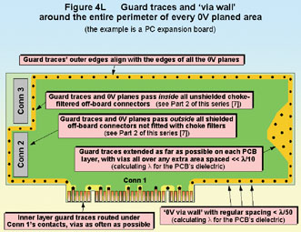
The example in Figure 4L is for a PCB with a single overall 0V plane. Where split 0V planes are used, each plane area should have a via wall around it (as shown in Figure 4L) so some of the ’perimeter guard traces’ and their via walls will now lie inside the PCB’s overall perimeter.
Areas of circuitry with separate 0V planes are — of course — ’segregated circuit zones’ as described in Part 2 of this series [7] and any conductors interconnecting them, whether wires or traces, should be treated as [7] recommends. Please note that split 0V planes are not generally recommended these days — this is discussed in detail in section 3 below.
Instead of a via wall, some designers use ‘PCB edge plating’ to link the guard traces and 0V planes together around the perimeter of the 0V planes. This uses the ‘de-smearing’ PCB fabrication technique that plates the barrels of the through-holes and vias, to plate the edges of the PCB as well. Some companies edge-plate with no problems, whilst others have difficulty, so it seems that not all PCB manufacturers have equal skills or processes.
2.11 Locating via holes for aggressive signals or power
The return currents associated with via holes excite the cavity resonances in plane pairs. This is one reason why it is important to route all of the most aggressive signals (e.g. clocks, strobes, etc.) on a single PCB layers, as far as possible (described in more detail in Part 7 of this series).
But the excitation caused by via hole currents can be minimised, improving EMC, by locating these via holes at the places where the plane pair resonance causes a low impedance to occur at the cavity resonant frequency of concern [14]. For simple plane shapes, determining where these low-impedance points occur can sometimes be done by inspection and simple mathematics (see above) – but complex plane shapes will require a computer simulation of the PCB, or experiments with a test board.
For the best EMC, the most aggressive signals should generally be routed as striplines, which are sandwiched between two planes (described in Part 6 of this series). If these striplines are kept on a single layer, they will only have to change layers at their ends to connect to the devices soldered to the outer layers of the PCB. So to improve EMC the devices that drive these aggressive traces should be placed at the places where the cavity resonances cause low impedances.
2.12 When traces change layers
The RF plane return currents associated with traces (see Figure 4A) are forced by ‘skin effect’ to flow in the surface of the plane that is closest to the trace. When traces change layers, their surface RF return currents cannot flow through the thickness of the plane. So where a trace becomes routed against the other side of the same plane, its return current will flow to the other surface around the rim of the antipad in the plane created by the via hole for the trace.
Where a trace becomes routed against a different plane at the same voltage (usually 0V) the interplane capacitance is insufficient to make a good connection – so a via hole should be added to link the two planes together very close (i.e. < 3mm) to the trace’s layer-change.
But where a trace becomes routed against a plane with a different voltage, it is important to fit a decoupling capacitor between the two planes, very close (i.e. < 3mm) to the trace’s layer-change. The return current will pass through the decap, so the value and type of decap, and its self-resonant frequency, should be chosen to suit the spectrum of the signal.
As will be discussed in Part 6 of this series, adequately controlling the return current path for very high-speed signals for good EMC may require no layer changes along the length of a trace, except for the connections to the devices at either end of the trace. This often leads to an increase in the number of plane layers.
2.13 Component-side planes for DC/DC converters and clocks
Transient currents in DC/DC converters can be very intense and even in the low impedances of an unbroken 0V plane can give rise to significant amounts of noise, possibly due to the resistance of the plane. So most DC/DC manufacturers recommend a separate very small component-side 0V plane for the DC/DC components, that is only connected to the main 0V plane at one point by a single large-diameter via (or by a number of smaller vias grouped closely together).
3 Splitting a 0V plane is not generally a good idea any more
Never split a 0V plane just because ‘we always used to do it’, or because any EMC guideline or IC application note says so. It used to be traditional to split planes between analogue and digital areas, but the author has found on hundreds of PCB designs since 1981 that PCBs can generally be designed to have better signal quality and EMC by using one 0V plane for all the circuits. Many other electronic designers have found the same. It is not unusual for analogue signal quality to be significantly better than what had previously been considered for decades to be the state of the art.
Due to the small silicon processes used in modern ICs, split 0V planes should now only be used as part of a well thought-out EMC plan, implemented by people who are sufficiently EMC-competent and equipped with all necessary EMC tools. 0V plane splits of any practical width don’t work well as splits above 1GHz anyway, and hardly have any effect >2.5GHz, due to the reducing impedance of the stray capacitance across the split as frequencies increase.
The problem is that – for traces that must cross a 0V plane split – it is very important indeed to maintain the intimate proximity of the send and return currents. This is not always easy, or low-cost, but if it is not done correctly the resulting degradation in EMC will be much worse than the benefits that could ever be hoped to be achieved by the use of a split. How to deal with traces that cross plane splits is discussed in the next section.
One way of dealing with uncertainty over whether to split a 0V plane or not, is to construct a prototype PCB designed to provide both options, then test it to see what works best.
Because the circuit has been laid out on the PCB in segregated circuit zones, as described in [7], it is easy to split the 0V plane between these zones. Then pad patterns that can be used for small capacitors, resistors or zero-ohm links should be placed at regular intervals around all the perimeters of all of the plane splits, so that they can be used to connect between the planes on either side of the split. These are often called ‘plane stitching’ components, and Figure 4M shows the general idea.

The spacings between the plane stitching components, around the perimeter of a split, should not exceed λ/10 at the highest frequency of concern (calculating λ taking the PCB dielectric’s k into account). So, for example, to control up to 1GHz in an FR4 PCB, the spacing between the stitching components should be no greater than 15mm.
The prototype PCB should employ as near to the final circuits and software as possible, and be tested for signal quality (analogue), SI and EMC, starting off with no stitching components fitted at all (except for any zero-ohm links used to connect to each plane at a single location, if this is not already done with traces). There is no need to apply full EMC testing as if for a final product – it is often possible to test emissions well enough on an ordinary laboratory bench using close-field probes and a low-cost or hired spectrum analyser. See [15] for close-field probe construction details.
Capacitors of various values (usually in the range 1-100nF) are then fitted to some or all of the stitching pads to see if the functional performance is improved and emissions reduced (or immunity improved). A single plane connection at d.c. plus capacitive stitching can be regarded as a hybrid plane bonding scheme, rather like the hybrid chassis bonding scheme discussed in [8]. Zero-ohm links can also be fitted at some or all of the stitching pads, and if resonance is suspected it might be worthwhile trying some resistors (or series resistor-capacitors) instead.
It should be borne in mind that unless all of the stitching components are fitted, adequate control of SI and emissions may not be achieved at the higher frequencies of concern. In some cases adding a few stitching components might make some emissions worse, but adding more might make it better than the initial result.
The alert reader will, of course, have spotted that the range of possible stitching experiments is enormous. Most designers will try a few obvious alternatives, for example…
- all stitching pads fitted with zero-ohm links
- all stitching pads fitted with capacitors, using 1, 2.7, 4.7 and 10nF devices in turn around each perimeter.
Then they will iterate depending on which gave the best results compared with the initial experiment with only the essential d.c. plane connections.
Although the author prefers not to split 0V planes at all, there are some instances where it is essential, for example where there is a galvanically isolated circuit zones sharing a PCB. In this situation the galvanically isolated area of 0V should be stitched to the main 0V plane with a number of small capacitors spread around the perimeter of the split according to the above rules, as shown in Figure 4N.
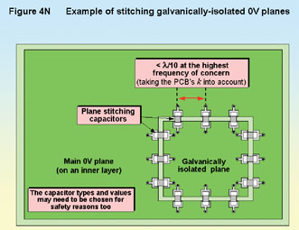
The plane split provides the necessary galvanic isolation at d.c. and powerline or even audio frequencies, and the stitching capacitors approximate (as best as they can) the benefits of an unbroken 0V plane over the whole PCB at RF. The stitching capacitors often need to be high-voltage types. Where safety is an issue, the types and values of the capacitors will usually need to be chosen for safety as well as for EMC reasons.
4 When traces must cross a 0V or power plane split
Where possible, never allow a trace to cross a plane split because it is difficult to control the trace’s return RF currents (which flow in the surface of the adjacent plane or planes) so as not to cause EMC problems. Some designers think that low-frequency analogue signals or power have no RF content so there is no need to worry about the RF return currents for such traces, but such signals and power are always vulnerable to RF interference, so the same PCB EMC design techniques should be applied.
In any case, any product that employs switch-mode power conversion (e.g. DC/DC converters) or clocked digital circuits (e.g. a microcontroller) has common-mode RF currents flowing in all of its traces, whatever the type of signal or power they are intended to carry. Common-mode currents are the major cause of EMC problems, so all of the EMC techniques described in this series apply to all traces, unless otherwise noted.
Issues concerning the splitting of 0V planes were discussed in the preceding section, and 0V planes should only be split as part of a well-thought-out EMC plan. But power planes are often split, and the best way to deal with traces that would have to cross power plane splits is to add an unbroken 0V plane between the traces and the power plane layer.
But if you must cross a split with a trace – you must provide a return path as physically close to the send path as possible, even if this creates a short-circuit across the split. At the frequencies of concern for EMC these days it is much more important to keep the return current path intimately associated with the send path, than it is to employ split planes.
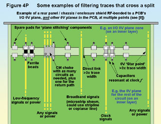
To help maintain the purpose of the plane’s split without worsening EMC too much, the send and return current paths for each trace must be filtered so they are band-limited to suit the wanted signal (or fitted with a CM choke). This allows the split to continue to provide isolation at other frequencies. Figure 4P shows a number of examples of filters fitted in send and return paths crossing a split, but only the series element of each filter that crosses the split is shown, to make the figure easier to read.
Where the bandwidth must be the highest and no filtering is possible, the return path must be a trace at least three times wider than the signal trace (see figure 4A), on an adjacent layer, centred under the signal trace. Closely-coupled differential transmission lines are the least affected by crossing plane splits. Coplanar transmission lines can be used instead, for single-ended or differential lines. For more on transmission lines, see Part 6 of this series.
CM chokes wind both the send and return current paths in the same direction on a magnetic core. They have little effect on the differential-mode (DM) current (the wanted signal) but put an impedance in the path of the CM current. Consequently CM chokes are ideal for use when signals must cross plane splits — they have very little filtering effect on the DM signals’ send and return current paths — and they help maintain the purpose of the split. CM chokes are now available in a wide var