Advanced PCB design and layout for EMC - Part 5 Decoupling, including buried capacitance technology
This is the fifth in a series of eight articles on good-practice design techniques for electromagnetic compatibility (EMC) for printed circuit board (PCB) design and layout. This series is intended for the designers of any electronic circuits that are to be constructed on PCBs, and of course for the PCB designers themselves. All applications areas are covered, from household appliances; commercial, medical and industrial equipment; through automotive, rail and marine to aerospace and military.
These PCB techniques are helpful when it is desired to…
- Save cost by reducing (or eliminating) enclosure-level shielding
- Reduce time-to-market and compliance costs by reducing the number of design iterations
- Improve the range of co-located wireless datacomms (GSM, DECT, Bluetooth, IEEE 802.11, etc.)
- Use very high-speed devices, or high power digital signal processing (DSP)
- Use the latest IC technologies (130nm or 90nm processes, ‘chip scale’ packages, etc.)
The topics to be covered in this series are:
- Saving time and cost overall
- Segregation and interface suppression
- PCB-chassis bonding
- Reference planes for 0V and power
- Decoupling, including buried capacitance technology
- Transmission lines
- Routing and layer stacking, including microvia technology
- A number of miscellaneous final issues
A previous series by the same author in the EMC & Compliance Journal in 1999 “Design Techniques for EMC” [1] included a section on PCB design and layout (“Part 5 – PCB Design and Layout”, October 1999, pages 5 – 17), but only set out to cover the most basic PCB techniques for EMC – the ones that all PCBs should follow no matter how simple their circuits. That series is posted on the web and the web versions have been substantially improved over the intervening years [2]. Other articles and publications by this author (e.g. [3] [4] and Volume 3 of [5]) have also addressed basic PCB techniques for EMC. This series will not repeat the basic design information in these articles – it will build upon it.
Like the above articles, this series will not spend much time analysing why these techniques work, they will focus on describing their practical application and when they are appropriate. But these techniques are well-proven in practice by numerous designers world-wide, and the reasons why they work are understood by academics, so they can be used with confidence. There are few techniques described in this series that are relatively unproven, and this will be mentioned where appropriate.
Table of Contents, for this Part of the series
1Introduction to decoupling
2 Decoupling with discrete capacitors
2.1 Which circuit locations need decaps?
2.2 The benefits of decaps in ICs and MCMs
2.3 How much decoupling capacitance to use?
2.4 Types of decaps
2.5 Layouts that reduce the size of the current loop
2.6 Series resonances in decaps
2.7 Using ferrites in decoupling
2.8 Splitting the decap into two
2.9 Using multiple decaps in parallel
2.10 Other ways to reduce decap ESL
3 Decoupling with 0V/Power plane pairs
3.1 Introduction to the decoupling benefits of 0V/Power plane pairs
3.2 The distributed capacitance of a 0V/Power plane pair
3.3 PCB 0V and power routing with 0V/Power plane pairs
3.4 Defeating parallel decap resonances when using 0V/power plane pairs
3.5 ‘Cavity resonances’ in 0V/power plane pairs
3.6 Bonding planes with decaps to increase resonant frequencies
3.7 Power plane islands fed by π filters
3.8 Damping cavity resonance peaks
3.9 The spreading inductance of planes
3.10 The 20-H rule
3.11Taking advantage of decap series resonances
3.12 Decap walls
3.13 Other 0V/Power plane pair techniques to reduce emissions
3.14 The buried capacitance technique
4 Field solvers for power bus impedance simulations
5 EMC-competent QA, change control, cost-reduction
6 Compromises
7 References
1. Introduction to decoupling
We need very low impedances in the power distribution networks (‘power busses’) that provide DC voltages to the devices on our PCBs, so that the fluctuating current demands of the ICs and transistors don’t cause excessive emissions of electric and/or magnetic fields. These fluctuating currents are caused by…
- Stray capacitances associated with the loads on the signals
- Shoot-through currents in totem-pole drivers
- Core (processing) noise
These three sources of current ‘noise’, and the resulting voltage noise created as they flow through the power bus impedance, are shown by Figure 5A.

‘Stray’ capacitance is unavoidably associated with all signal loads (e.g. an input to a CMOS IC or an operational amplifier) due to device terminals, lead frames, bond wires, and the capacitance associated with the internal semiconductor features. To this must be added the stray capacitance of the traces and pads of the PCB itself. The capacitances involved are quite small, often just a few tens of pF in total. As the transition time of digital signals continues to decrease (see Part 1 of this series [6]) the transient currents created by charging and discharging the capacitances associated with a load increase, increasing the levels of the emissions from the power busses.
‘Shoot-through’ currents are created by totem-pole type driver circuits, at the instant of their switching. For a very brief time, both the upper and lower transistors in the totem pole are ‘on’ together, momentarily shorting out the power bus. It is possible to design totem-pole driver circuits so that the conduction times of the upper and lower devices do not overlap, and this is often done in high-power switch-mode converters to prevent actual device damage from the very high currents that flow when the power bus is short-circuited, but it not typically done in digital ICs. The inductance in the path of the resulting current limits the rate of rise of the shoot-through current, which would reach very high levels if the shoot-through period was not so short.
The shoot-through current of a modern 74HC glue logic device can exceed the current fluctuations caused by driving its output signals by as much as 15dB at frequencies above 30MHz. And despite its data sheet rise/fall time specification of 5ns (maximum) both of these noise currents can exist at significant levels at frequencies up to (and maybe beyond) 600MHz.
The inductances associated with the power bus inside an IC cause voltage noises (with respect to the PCB) to appear on its internal 0V and power voltage references. These noises are called ‘ground bounce’ and ‘rail bounce’ (sometimes: ‘rail collapse’). Because these noises occur on all of the IC’s input and output pins they contribute to the common-mode noise emissions from a device and from the PCB it is mounted on. It can be important for good EMC performance of a PCB to design or select ICs to have a low ground-bounce and rail-bounce, but device selection is not a subject of this series of articles (see [1] or [2] instead).
Core noise is a feature of VLSI ICs, such as microprocessors and large FPGAs, which have a core of semiconductors operating at very high speeds. These internal circuits have to drive signals into internal capacitive loads, can suffer from shoot-through currents, and their transient current demands add to an IC’s overall current fluctuations. The frequencies of core noise currents are usually much higher than those from the other two causes, for example: the core of some Xilinx FPGAs can have power current demands with 50ps durations – equivalent to a noise frequency spectrum that extends to at least 13GHz.
Magnetic field emissions are dealt with by making the areas enclosed by the DC power current loops as small as possible. Where the 0V and power is supplied by traces, these traces must be as close together as possible, usually achieved by routing 0V and power traces side-by-side or broadside along their whole route.
But Part 4 of this series [7] showed how important a PCB 0V plane is for EMC, for a variety of reasons, and when we have a 0V plane we achieve a small current loop by routing DC power ‘bus’ traces (often called power busses or power rails) on a PCB layer that is adjacent to a 0V plane. Closer layer spacing means smaller loop areas and lower emissions.
[7] also mentioned the use of a 0V/Power plane pair, in which both the 0V and power distributions use planes, on adjacent layers. Using this technique in a PCB stack-up achieves the minimum possible current loop area. Closer 0V/Power plane spacing means even smaller loop areas and lower emissions of magnetic fields.
Electric field emissions are dealt with by making the impedance of the power bus – at the point of connection of the IC or transistor that is drawing fluctuating currents – as low as possible at all of the frequencies of concern. This aims to reduce the magnitude of the fluctuating voltages created by the fluctuating DC currents, because smaller voltage fluctuations will give rise to lower electric-field emissions. The classical way of achieving a low impedance at the point of connection is to fit a capacitor there – known as a decoupling capacitor, or decap. Also, closer spacing of the power bus and its 0V return reduces the amount of electric field emitted, for a given power bus noise voltage.
The distributed capacitance of a 0V/Power plane pair is another way of achieving a low power bus impedance, aided by the low DC resistances of planes (versus traces) and also by the high mutual inductance between the two adjacent planes. Closer 0V/Power plane spacing generally means lower power bus impedances.
Unfortunately, decaps are not perfect capacitors and 0V/power plane pairs can cause problems if not designed carefully – as a result, effectively decoupling modern PCBs can be a difficult task. The rest of this article explores these issues and how they are overcome at present. It then goes on to describe the buried capacitance technique that – along with HDI (see section 5 of Part 4 [7] and Part 7 of this series) – will no doubt be as ubiquitous and ‘normal’ in a few year’s time, as FR4 and through-hole-plate (THP) PCBs are today.
Bypassing is another word for decoupling, and bypass capacitors another description for decoupling capacitors. This series does not use the ‘bypass’ words – partly because ‘decap’ is a nicer abbreviation than ‘bypasscap’.
2. Decoupling with discrete capacitors
Unless otherwise stated, this section of this article assumes a 0V plane with low impedance at the highest frequency of concern (see [7] for design details) – and power distribution using thin traces.
2.1 Which circuit locations need decaps?
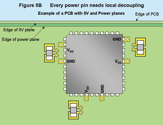
Because of the very high switching speeds now achieved by digital ICs due to the continual die-shrinking by the semiconductor industry (“Moore’s Law”), decaps are now required at every power pin of every IC (even old-fashioned glue logic) as shown by Figure 5B.
And to improve emissions and immunity performance decaps are also required at least at every other location on the PCB where fluctuating currents are drawn from a power bus, whether the circuits are digital, analogue, radio-frequency, or switch-mode.
Whichever DC voltages they are connected to, all decaps should connect to the 0V plane used by the circuit their device is a part of. (See [7] for more on 0V planes, including what to do with a galvanically isolated area of 0V plane).
It also helps EMC to fit decaps near to every off-board connector, whether they carry signals or power. And fitting decaps to the voltage reference nodes of operational amplifier and comparator circuits, and the voltage reference pins of A/D and D/A converters, can also help improve functionality and improve immunity to EMI.
2.2 The benefits of decaps in ICs and MCMs
The most effective decoupling per pF of decap is achieved by silicon nitride decaps actually created in the silicon die of an IC itself. The next most effective use of decap pF is mounting decaps in an IC’s package (‘hybrid circuit’ construction) – and mounting decaps on a multi-chip module (MCM), as is done with Pentium IV™, is the next in effectiveness.
The above three decap locations are the most effective at controlling the very highest frequencies because they achieve the smallest possible size of current loop. So when choosing devices or designing FPGAs or ASICs or MCMs it will greatly ease the design (and cost) of the PCB power bus decoupling if as much decoupling capacitance as possible is embedded in the silicon chips or on the MCMs themselves.
It is very important that the discrete decaps used have the very lowest ESL – such as is achieved for example by AVX’s IDC and LICA devices, and X2Y® devices (see section 2.4). Going any further with this topic would be outside the scope of this article.
2.3 How much decoupling capacitance to use?
The basic functional reason for decoupling digital ICs is to maintain the voltage rail within certain specified tolerances despite their fluctuating current demands. It is easy to calculate the amount of decoupling capacitance C required for an IC using the expression CΔV = IΔt.
ΔV is the maximum permitted reduction from the actual power bus voltage, in Volts, that will still permit the IC to function correctly – and is easily calculated from the worst-case power bus voltage (taking into account regulator initial tolerances, temperature coefficients and operating temperature ranges, ageing coefficients, the voltage drop due to the resistance between the power bus and the IC, plus the minimum operating voltage specification from the IC’s data sheet). I is the maximum current demand in Amps and Δt is the time this demand exists for. The problem is that it is difficult to specify IΔt for modern VLSI devices because it is a fluctuating quantity that depends on the operational mode of the device and the loads it is driving. But it may be possible to measure an IC’s transient current demands with a high-frequency current probe, when the IC is operating in representative worst-case conditions.
It often turns out that 10nF is sufficient for decoupling glue logic, but most VLSI devices will need more and their manufacturers will usually recommend how much. For example, Xilinx [8] recommend using much more than 1/m times the ‘equivalent switched capacitance’ (where m is the maximum percentage variation permitted in the power bus voltage at the IC’s power pin). Equivalent switched capacitance is defined as P/fV2 (where P = the total wattage consumed by the IC; V = its DC supply voltage; f = its clock frequency).
Xilinx say that once the equivalent switched capacitance has been determined, it is multiplied by much more than 1/m to find the total capacitance required by the IC, then this total is divided by the total number of power pins connected to the same power bus to find the value of capacitance to be placed near each of the pins connected to the power bus in question.
A significant problem is that the type of decap used and/or the inductance in the current loop formed by the decap and its associated IC, could prevent the decap being effective when there are fast fluctuations in device power bus current. As a result, good VLSI manufacturers generally provide a wealth of data on how to decouple their devices (for example, [9] from Xilinx).
Our discussion on decoupling in section 2.3 has so far concerned decoupling for reliable functionality, but decoupling to improve EMC performance at PCB-level is much more difficult. So please be aware that IC manufacturers’ application notes and other decoupling advice might not be as good as the very up-to-date EMC practices described in the rest of this article.
2.4 Types of decaps
The best decoupling capacitors are surface-mounted multilayer ceramic (MLCC), because ceramic dielectrics are true electrostatic barriers (charge separation devices) that can release all their charge at whatever rate is required. In practice, their rate of discharge is limited by the self-inductance (‘equivalent series inductance’, or ESL) of the device and the inductance in its external circuit (which are also limitations for all other types of capacitors). MLCCs especially designed for high frequencies exist, such as the Murata GRH700 series, and some designers prefer to use them, but because they are not purchased globally in very high volumes they are more costly than ordinary MLCCs.
Plastic dielectrics suffer from dielectric absorption, which means that not all of their stored charge is available instantaneously. Some dielectrics (e.g. Teflon, polycarbonate) are better than others, but they are more costly and the commonplace low-cost polyester dielectric gets progressively worse as frequencies increase above a few MHz. Plastic decaps also tend to have higher ESLs than MLCCs, due to the way they are constructed.
Electrolytic capacitors, including solid tantalum, rely on chemical changes to store their charge, and until recently have been valued for having a higher charge storage density than plastic or ceramic types. Having to wait for chemical changes to happen in them before the charge is released restricts their practical use to frequencies under 1MHz. Electrolytics also tend to have higher ESLs than MLCCs, due to their internal construction.
Recent years have seen significant advancements in MLCCs, with 100nF now available from some suppliers in the very good X7R and/or Z5U dielectrics in the extremely small 0201 package size. The lower internal impedances of MLCCs can enable them to do as good a job of decoupling lower frequencies as electrolytics that have values up to 5 times larger, so a 100nF MLCC can sometimes replace a 470nF electrolytic. The only reasons for using electrolytics these days are decoupling high voltages, or where lowest cost is more important than size, weight, and reliability.
A decap’s ESL is an important contributor to the inductance of the current loop consisting of the decap, the IC it is associated with, and the interconnection between the two – see Section 2.5 and Figure 5C below. It is very important to reduce the inductance of this current loop, and so it is very important to use decaps with low ESLs.
Smaller and/or lower-profile surface-mounted MLCCs tend to have lower ESLs. Standard three-terminal feedthrough capacitors can be used to achieve lower ESL, and X2Y Attenuators are another recent development in low-ESL decaps, and both are discussed in more detail in section 2.10 below.
‘Reversed aspect’ MLCCs have their metallised terminals along their long edges – instead of on their short edges (as is more usual with surface mounted capacitors) and this reduces their ESLs. For example, 0508 and 0306 styles indicate a reversed aspect package (instead of the more usual 0805 and 0603 styles). AVX say that an 0805 MLCC has an ESL of around 1nH, whereas an 0508 has around 400pH and 0306 around 325pH [10].
AVX also offer ‘interdigitated capacitors’ (IDC) and ‘low inductance chip arrays’ (LICA), which offer much lower ESLs than reversed aspect decaps. For example, [10] says that an 0508 IDC has an ESL of under 100pH, whereas LICA (which uses a ball-grid array package style) has under 30pH.
2.5 Layouts that reduce the size of the current loop
To obtain the greatest reduction in magnetic and electric field emissions, the area enclosed by the current loop created by the decap and the device it is decoupling must be minimised.
Since this series is about advanced EMC techniques in PCBs, this article assumes that a high-integrity 0V plane (at least) is used in the PCB (see [7]). Figure 5C shows the schematic of the current loop that we are concerned with, and Figure 5D shows a suitable layout.

As was mentioned earlier – the complete power current loop between decap and IC is important – and this includes the lead frame, bond wires, and silicon of the IC. Since we often don’t know the path taken by the power current inside the IC, this article ignores it. But when choosing devices or designing FPGAs or ASICs it is important to ensure that the inductance created by its internal power bus does not prevent the PCB designer from decoupling well enough to achieve good EMC performance at the PCB level. Some Ball Grid Arrays (BGAs) have many hundreds of pins dedicated just to 0V and power connections exactly for this purpose. Lo-profile ICs (such as BGAs) and/or ICs which include internal 0V planes, will generally be an aid to PCB decoupling. IC sockets should, in general, not be used because the inductance they add between IC and decap prevents PCB decoupling from being effective for EMC purposes.
The inductance of simple two-dimensional shapes of current loops can easily be calculated using standard equations – but they are not given here because it is much quicker to use on-line calculators generously provided free on the Internet [11]. Real decap-IC current loops are usually three-dimensional, and the inductance of the complex shapes they create can be hard to determine without a field solver (see later). Methods of reducing the inductance of the decap-IC current loops – and the internal inductance of the discrete decaps – are covered during the rest of this article.
The minimum decap-IC current loop inductance is achieved by choosing a decap with a low value of ESL, and minimising the inductance of the interconnections to its IC (or other device). In the case of a 0V plane and power trace – the layout that achieves the minimum interconnect inductance is shown by Figure 5D.

The power terminal of the decap shares the same pad as the power pin of the IC, with minimum spacing between IC and the decap. The 0V plane should be the next layer down from the surface layer where the components are mounted, and all components should connect to it using the shortest widest traces (via-in-pad where practical). Closer spacing of the 0V plane to the component side of the PCB will reduce the interconnect inductance further. To help the decap remove noise from the power bus, it helps if the current from the power supply has to flow across the pad of the decap to get to the IC.
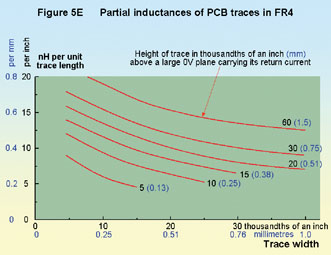
To help with the design of the layout for a decap, Figure 5E shows how the partial inductance of a trace routed over an adjacent 0V plane varies with trace width and spacing from the plane.
Where it is not possible to share the same pad because the decap has to be moved further away from the power pin for some reason, it is best to minimise the decap’s interconnect inductance by employing a small copper area (a small power plane) instead of a trace between the IC and decap as shown by Figure 5F. As before the 0V plane must lie on the layer adjacent to the small power plane, and closer spacing between these two layers will reduce the interconnect inductance.
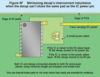
The reason for specifying the layer that is used for the 0V plane is that the decap’s interconnect inductance is significantly reduced by maximising the mutual inductance between the ‘send’ and ‘return’ currents, by placing them on adjacent layers. Closer spacing of these layers increases their mutual inductance, and this reduces the overall loop inductance. This issue is discussed in more detail in section 3 below.
To help reduce the area of the current loop on PCBs with 0V and power planes – where the IC to be decoupled is closest to its 0V plane layer its decap should be placed close to its power pin(s). But if the IC is closest to the layer on which its power trace or plane is routed, its decap should be placed close to its 0V pin(s).
To help achieve low power bus impedance, some manufacturers embed decaps inside their PCB itself. Some do this by making parallel plate capacitors out of copper areas and small areas of special insulating material with a high dielectric constant. Some others do it by milling an oval hole in the PCB, plating its ends, and soldering a discrete decap inside the hole. These are both expensive and/or problematic techniques that are not recommended for general use.
The reduction of the areas or volumes enclosed by the decaps’ interconnects is important for all types of circuits, not just digital. When decoupling analogue circuits, the basic issues for decoupling are usually stability, rejection of power supply noise, and immunity to EMI. Opamps used for low-frequency instrumentation and audio circuits usually employ 100nF multilayer ceramic decaps at each power pin, whereas high frequency and RF devices might need to employ 10nF or even 1nF for stability, and might need to employ similar techniques to those described below to maintain a low power bus impedance over a wide range of frequencies.
2.6 Series resonances in decaps
All decaps have ESL which, in combination with the inductance of their decap’s interconnect (see Figure 5C), causes them to behave as a series resonant circuit.
Series resonant circuits have a Self Resonant Frequency (SRF) at which their impedance falls to a minimum (limited only by resistance in the circuit). fSRF = 1/2π√(LTOTC), where LTOT = the total inductance associated with the decap (the ESL of the capacitor plus the decap’s interconnect inductance, see Figure 5C). LTOT in Henries (H) and C in Farads (F) gives fSRF in Hz. Above the fSRF the decap impedance is simply 2πfLTOT, so it increases with increasing frequency. Figure 5G shows the series resonant behaviour of some example decaps, assuming average 0805 or 0603 decaps with an ESL of around 1nH, plus a good pad pattern (from Figure 4H of [7]) that achieves an LTOT of 2nH.

The dotted lines in Figure 5G shows how we might expect an ideal decap’s self-impedance to continually decrease with increasing frequency, assuming no inductance in the current loop at all. But the solid lines show that, at their SRF, real decaps can have an impedance that is lower than that of an ideal capacitor of the same value. Figure 5G also shows that at frequencies above their SRF, decap impedance is totally defined by LTOT.
Modern ICs switch so quickly that they generate significant levels of emissions at frequencies above 300MHz, and so Figure 5G shows us how very important it is to minimise LTOT, to try to reduce the power bus impedance at such high frequencies.
The rest of this article includes design techniques to overcome the problem of inductance in power bus decoupling.
2.7 Using ferrites in decoupling
Wherever the impedance of the portion of power bus closest to a device (such as an IC) is not low enough, noisy currents will tend to circulate around the PCB’s whole power bus, including any wires connecting to an off-board DC power supply, and this will increase emissions.
Adding a ferrite bead between each power pin and its power supply, as shown by Figures 5H and 5J, can reduce emissions by increasing the RF impedance of the power supply in such a way that more of the noise current remains local to the decap/device combination. As long as the longest dimension of the current loop between the decap and the IC remains smaller than one-quarter of a wavelength (λ), the emissions will then be less than they would be without the ferrite. (λ/4 for 1GHz in FR4 is 37mm.)

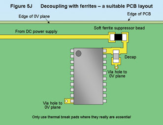
The ferrite beads used for this purpose should be RF suppression devices, not inductors wound on ferrite cores, no matter how small. It is often possible to choose specific types of ferrite beads that are more effective than others at the emissions (or immunity) frequencies of concern.
The ferrite bead-decap combination can be thought of as a low-pass filter that helps to keep noisy currents from an IC out of the main power bus. When this technique is used it may be found that only some of the ICs need ferrites in their DC rails — for example: clock generators and clock buffers. It may also be found that some IC cannot use ferrites in their power bus because the resistance is too high (check with the IC manufacturers’ application notes).
However, simply adding a ferrite as shown above will cause the impedance of the power bus as seen by the IC will rise, so it will suffer from higher values of supply noise (rail bounce). With some ICs this can cause functional problems, so ferrite decoupling may require the use of higher values or higher specification decaps (see 2.8, 2.9, 2.10 and section 3 below).
2.8 Splitting the decap into two
A decap in combination with the stray impedances of a power bus can be thought of as a filter. A problem with single-capacitor filters is that the current loops associated with the input and output sides of the filter share a common boundary – the capacitor – enabling the magnetic flux associated with the input loop to couple quite well with output loop (and vice-versa). The resulting mutual inductance between the filter’s input and output circuits reduces the attenuation it achieves in real life.
One way to deal with this problem is described by [12], and was also used in Part 2 of this series [13]. Two decaps are used along a power trace, spaced as far apart as possible – but no further apart than one-tenth of the wavelength in the PCB dielectric at the highest frequency of concern (see Figure 2V of [13]). The wavelength is given in meters by 300/f√k where f is the frequency in MHz and k is the relative dielectric constant of the PCB substrate (the term εr is often used instead of k). The k for FR4 is nominally 4.0 at frequencies above 1MHz, so for a top frequency of 300MHz with an FR4 dielectric in the PCB – the maximum spacing between the two decaps would be 50mm.
Providing the component placement and trace routing is done carefully, so as not to compromise the physical segregation achieved between these two loops, the mutual inductance between the input and output current loops is considerably reduced. The restriction of the spacing between the two decaps to <λ/10 prevents the newly-created current loop between the two decaps from becoming resonant – as this would once again couple the input and output loops very closely. Clearly, this technique could also employ three or more decaps in series along a power trace to get even better noise filtering.
2.9 Using multiple decaps in parallel
Using a number of decaps in parallel is one way of reducing the effect of their ESL. But this only has a significant overall benefit if the inductance of the decap’s interconnect is much smaller than the ESL of a single decap (see section 2.4 and its figures above). Since it can be difficult to share an IC’s power pin pad with more than one decap, the scheme of Figure 5F is often used with all the decaps to be paralleled sharing the same small power plane.
When n identical decaps are paralleled the impedance they achieve is reduced. The reduction depends on their layout with respect to one another, but 1/n times the impedance of a single decap can be achieved. So 10 decaps with the same ESL can be arranged to have 1/10th the impedance of just one decap.
The most obvious way of arranging multiple decaps is to place them in a bank, side-by-side, with all their 0V connections at the same end – but this would not create the impedance reduction required. Since their current flows are in the same orientation, and the devices are close enough to have significant mutual inductance, the reduction in overall impedance is not as much as 1/n. With such a regular layout, the devices should be far apart to minimise their mutual inductance and hence minimise their overall impedance, as shown in Figure 5K.
However, the devices can be placed close together if they are arranged so that the magnetic fluxes, created by the current flowing through their bodies, cancel. Figure 5P below shows an example of this technique with just two decaps. Figure 5K shows how this technique might be applied when using five decaps, but if you are planning on using this technique take care not to infringe Dell Patent #6,337,798.

It is claimed that a bank of X2Y® Attenuators used as decaps (see section 2.10) can be closely spaced together in the same orientation without their mutual inductance compromising their overall effect, but this requires identical and symmetrical locations for the 0V via hole(s) for each device.
At the time of writing there are two conflicting recommendations on the values to use when paralleling decaps – some experts recommend using identical values whilst others recommend using a variety of values. But all of them agree that it is essential to choose decaps with the smallest ESLs and to minimise the inductance in the decaps’ interconnections.>/p>
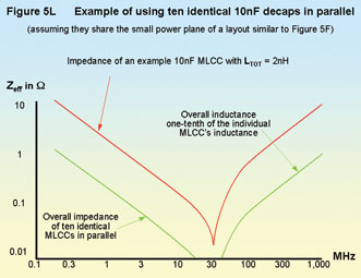
Figure 5L shows the effects of using ten identical 10nF decaps – assuming they share the small power plane of a layout similar to Figure 5F and assuming they are laid out optimally to achieve 1/n improvement in overall ESL (see Figure 5K).
Using identical types and values of decaps avoids the problems of parallel resonances that occur when decaps with different SRFs are used. Figure 5M shows the sort of thing that happens when three different values of decap are paralleled under the same conditions as Figure 5L. In-between each pair of series resonant frequencies, a parallel resonance with a high impedance appears – not what we wanted.

The effects sketched in Figure 5M are easy to simulate using SPICE with simple models for the decaps that just include their capacitance values and ESLs, and many designers take this to be a good reason for not using different decap values in parallel. But it is possible to use a number of different values to achieve an overall power bus impedance that may give better overall performance than using identical values. The idea is to spread the series resonances around to get a lower impedance over a wider range, and choose values that are close enough together that the parallel resonances cannot achieve very high impedances.
Figure 5N shows an example of such a decoupling scheme using ten decaps with values ranging from 100 to 1nF (assuming they are laid out optimally to achieve 1/n improvement in overall ESL, see Figure 5K). The overall impedance of ten identical 10nF capacitors (from Figure 5L) is shown for comparison.

Figure 5N shows that using closely-spaced values of decaps we can achieve lower impedance over parts of the frequency range (in this example, below 12MHz and from 60 – 150MHz) with the trade-off of a higher impedance over part of the range (12-60MHz). Above about 150MHz the impedance is the same for both sets of parallel capacitors – simply equal to the impedance of 10 off 2nH inductors in parallel. For more on using multiple values of decap to extend the low-impedance frequency range, see [14].
When laying out the decaps for an IC using a variety of decap values, the decaps with the lower capacitance values should be placed closest to the IC’s power pin. It is often remarked that there is little value in using decaps with values below 1nF, but if their equivalent series resistances (ESRs) are low enough Figure 5N indicates that they may help achieve lower overall impedances at frequencies above 150MHz.
MLCCs with NPO or COG dielectrics tend to self-resonate at higher frequencies, for a given value of capacitance, which makes them more attractive for decoupling. But they have lower ESRs than the X7R and Z5U ceramic dielectrics usually used to pack much more capacitance into small decaps. Lower ESRs mean lower impedances at their SRFs, but the reduction in damping caused by the lower ESR losses makes the parallel resonance peak impedances higher. So in general it is better to avoid COG or NPO dielectrics and choose decaps with ESRs of 10mW or more. When using NPO or COG decaps their low ESRs make it very important to route them to their ICs in a way that achieves the lowest possible loop inductance. This helps reduce the amplitude of their parallel resonance peaks.
2.10 Other ways to reduce decap ESL
The ESL of a decap is caused by the flow of current within it. One way of reducing ESL is to place two decaps close together in an orientation such that the magnetic fluxes caused by their internal currents cancel each other out, as shown by Figure 5P (taken from [15], which in turn references [16]). Obviously, this technique can be applied to any number of decaps (see 2.9 above, and Figure 5K) – but if intending to use this technique, take care not to infringe Dell Patent #6,337,798.

Surface-mounted 3-terminal ‘feedthrough’ capacitors [17] and especially ‘X2Y® attenuators’, with one centrally located via (or two symmetrically located vias) to their 0V plane, have lower ESL than a similar size of 2-terminal capacitor. This is due to the magnetic field inside the capacitor being partially cancelled due to there being two current paths in opposite directions for at least part of their path through the body of the devices. The result is a higher SRF, and a lower impedance above the SRF, for a given capacitor value and package size. X2Y® attenuators have a special three-electrode internal structure that achieves better internal magnetic flux cancellation than a normal 3-terminal capacitor.
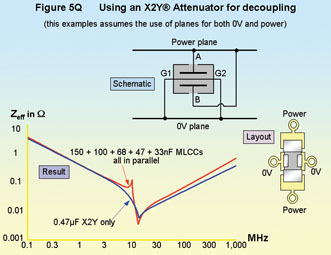
Figure 5Q shows a the schematic and pad pattern for an X2Y® attenuator when used with both 0V and power planes, plus a graph (from [18]) comparing the impedance of a 470nF X2Y device compared with that achieved by a parallel combination of five ordinary 2-terminal MLCC decaps (150 + 100 + 68 + 47 + 33nF). The graph shows that the single X2Y® has a better-controlled impedance curve and a lower impedance at frequencies above the SRF, implying that (in this example, at least) the X2Y® device and its interconnect achieves an inductance that is less than that of five MLCCs in parallel.
7. References
[1] Keith Armstrong, “Design Techniques for EMC” (in six parts), UK EMC Journal, Jan – Dec 1999
[2] Keith Armstrong, “Design Techniques for EMC” (in six parts), http://www.compliance-club.com/KeithArmstrongPortfolio
[3] M K Armstrong, “PCB Design Techniques for Lowest-Cost EMC Compliance: Part 1”, IEE Electronics and Communication Engineering Journal, Vol. 11 No. 4 August 1999, pages 185-194
[4] M K Armstrong, “PCB Design Techniques for Lowest-Cost EMC Compliance: Part 2”, IEE Electronics and Communication Engineering Journal, Vol. 11 No. 5 October 1999, pages 219-226
[5] “EMC and Electrical Safety Design Manuals”, a set of four volumes edited by Keith Armstrong and published by York EMC Services Ltd., 2002, ISBN 1-902009-07-X, sales@yorkemc.co.uk, phone: +44 (0)1904 434 440.
Volume 1 – What is EMC? ISBN 1-902009-05-3
Volume 2 – EMC Design Techniques – Part 1 ISBN 1-902009-06-1
Volume 3 – EMC Design Techniques – Part 2 ISBN 1-902009-07-X
Volume 4 – Safety of Electrical Equipment ISBN 1-902009-08-8
[6] Keith Armstrong, “Advanced PCB Design and Layout for EMC – Part 1: Saving Time and Cost Overall”, EMC & Compliance Journal, March 2004, pp 31-40, http://www.compliance-club.com/KeithArmstrongPortfolio.
[7] Keith Armstrong, “Advanced PCB Design and Layout for EMC – Part 4:Reference planes for 0V and power”, EMC & Compliance Journal, September 2004, pp 29- 42, http://www.compliance-club.com.
[8]Xilinx, “Powering Xilinx FPGAs”, Application Note ref: XAPP158 (v1.4) Feb 6, 2001, http://www.xilinx.com
[9]Xilinx, “Power Distribution System (PDS) Design: Using Bypass/Decoupling Capacitors”, Application Note ref: XAPP623 (v1.2) June 11, 2003, http://www.xilinx.com
[10]AVX, “Low Inductance Capacitors – Product Brochure”, available from: http://www.avxcorp.com/prodinfo_productdetail.asp?I=35 &ParentID=75 (or Google for ‘interdigitated capacitors’)
[11]For example the on-line inductance calculators kindly provided by the EMC Laboratory at the University of Missouri-Rolla at http://emcsun.ece.umr.edu/new-induct
[12]Theodore M Zeef, Todd H Hubing, Thomas P Van Doren, David Pommerenke, “Analysis of Simple Two-Capacitor Low-Pass Filters”, IEEE Transactions on Electromagnetic Compatibility, Vol. 45, No. 4, Nov 2003, pp 595-601
[13]Keith Armstrong, “Advanced PCB Design and Layout for EMC – Part 2: Segregation and interface suppression ”, EMC & Compliance Journal, May 2004, pp32-42, http://www.compliance-club.com/KeithArmstrongPortfolio.
[14]Douglas G Brooks, “ESR and Bypass Capacitor Self Resonant Behaviour – How to Select Bypass Caps”, UltraCAD Design Inc., available from http://www.ultracad.com.
[15]X2Y Attenuators LLC, “X2Y® Solution for Decoupling Printed Circuit Boards”, application note ref: Note# 1007, V 1.8, 8/26/03, available from www.x2y.com.
[16] Shim, Hwan H, Theodore M Zeeff, Todd H Hubing, “Decoupling Strategies for Printed Circuit Boards without Power Planes”, IEEE International EMC Symposium, 19-23 August 2002, Minneapolis, Minnesota, pages 258-261 in the symposium record.
[17]C N Olsen, T P Van Doren, T H Hubing, J L Drewniak, R E Dubroff, “Improving the High-Frequency Attenuation of Shunt Capacitor Low-Pass Filters”, IEEE International EMC Symposium, Montreal, August 13-17 2001, Symposium Record ISBN 0-7803-6569-0, pp 487-489.
[18]D L Sanders, J P Muccioli, A A Anthony, D J Anthony, “X2Y® Technology used for Decoupling”, IEE seminar, “New EMC Issues in Design: Techniques, Tools and Components”, Qinetiq, Farnborough UK, 28 April 2004, Seminar record: ISBN 0-86341-401-X, pp15-20, sales@iee.org.
I would like to reference all of the articles, papers, application notes and textbooks that back-up the techniques described in this series, but the reference list would take longer to write than this series! However, I must mention the papers presented at the annual IEEE International EMC Symposia organised by the IEEE’s EMC Society (http://www.ewh.ieee.org/soc/emcs), especially the dozens of wonderful papers by Todd Hubing and his staff and students at the University of Missouri-Rolla EMC Lab (http://www.emclab.umr.edu), and papers by Bruce Archambeault of IBM and the EMC experts at Sun Microsystems.
Many other contributors to the IEEE EMC Symposia, and other conferences and symposia and private correspondence are far too numerous to be named here, but the following stand out: Tim Williams of Elmac Services, http://www.elmac.co.uk; Mark Montrose of Montrose Compliance Services, http://www.montrosecompliance.com; John Howard, http://www.emcguru.com; Tim Jarvis of RadioCAD, http://www.radiocad.com; Eric Bogatin of Giga-Test Labs, http://www.gigatest.com; and dozens of application notes from National Semiconductor; Rambus Corp.; California Micro Devices; Intel; IBM; Cypress Semiconductor; Xilinx; Sun; Motorola; AVX; X2Y Attenuators; Giga-Test Labs; Ansoft and Flomerics. I apologise to the very many excellent people and companies that I have had to leave out of this list.
Some other useful textbooks are:
[A] Mark I. Montrose, “EMC and the Printed Circuit Board, design, theory, and layout made simple”, IEEE Press, 1999, ISBN 0-7803-4703-X
[B] Mark I. Montrose, “Printed Circuit Board Design Techniques for EMC Compliance, Second Edition”, IEEE Press, 2000, ISBN 0-7803-5376-5
[C]Howard W Johnson and M Graham, “High Speed Digital Design, a Handbook of Black Magic”, Prentice Hall, 1993, ISBN 0-1339-5724-1
[D]Howard W. Johnson, “High Speed Signal Propagation: Advanced Black Magic”, Prentice Hall, 2003, ISBN 0-1308-4408-X
Due to the length of this part of Keith’s series, we have split it into two and the rest of it will appear in the next issue 56 (January 2005).
Eur Ing Keith Armstrong C.Eng MIEE MIEEE Cherry Clough Consultants,
Member of: EMCTLA, EMCUK, EMCIA
keith.armstrong@cherryclough.com