Advanced PCB design and layout for EMC Part 6 - Transmission lines - 1st Part
This is the sixth in a series of eight articles on good-practice design techniques for electromagnetic compatibility (EMC) for printed circuit board (PCB) design and layout. This series is intended for the designers of any electronic circuits that are to be constructed on PCBs, and of course for the PCB designers themselves. All applications areas are covered, from household appliances; commercial, medical and industrial equipment; through automotive, rail and marine to aerospace and military.
These PCB techniques are helpful when it is desired to…
- Save cost by reducing (or eliminating) enclosure-level shielding
- Reduce time-to-market and compliance costs by reducing the number of design iterations
- Improve the range of co-located wireless datacomms (GSM, DECT, Bluetooth, IEEE 802.11, etc.)
- Use very high-speed devices, or high power digital signal processing (DSP)
- Use the latest IC technologies (130nm or 90nm chip processes, ‘chip scale’ packages, etc.)
The topics to be covered in this series are:
- Saving time and cost overall
- egregation and interface suppression
- PCB-chassis bonding
- Reference planes for 0V and power
- Decoupling, including buried capacitance technology
- Transmission lines
- Routing and layer stacking, including microvia technology
- A number of miscellaneous final issues
A previous series by the same author in the EMC & Compliance Journal in 1999 “Design Techniques for EMC” [1] included a section on PCB design and layout (“Part 5 – PCB Design and Layout”, October 1999, pages 5 – 17), but only set out to cover the most basic PCB techniques for EMC – the ones that all PCBs should follow no matter how simple their circuits. That series is posted on the web and the web versions have been substantially improved over the intervening years [2]. Other articles and publications by this author (e.g. [3] [4] and Volume 3 of [5]) have also addressed basic PCB techniques for EMC.
Like the above articles, this series will not spend much time analysing why these techniques work, it will focus on describing their practical applications and when they are appropriate. But these techniques are well-proven in practice by numerous designers world-wide, and the reasons why they work are understood by academics, so they can be used with confidence. There are few techniques described in this series that are relatively unproven, and this will be mentioned where appropriate.
Table of Contents, for this Part of the series
1 Matched transmission lines on PCBs
1.1 Introduction
1.2 Propagation velocity, V and characteristic impedance, Z0
1.3 The effects of impedance discontinuities
1.4 The effects of keeping Z0 constant
1.5 Time Domain Reflectometry (TDR)
1.6 When to use matched transmission lines
1.7 Increasing importance of matched transmission lines for modern products
1.8 It is the real rise/fall times that matter
1.9 Noises and immunity should also be taken into account
1.10 Calculating the waveforms at each end of a trace
1.11 Examples of two common types of transmission lines
1.12 Coplanar transmission lines
1.13 Correcting for capacitive loading
1.14 The need for PCB test traces
1.15 The relationship between rise time and frequency
2 Terminating transmission lines
2.1 A range of termination methods
2.2 Difficulties with drivers
2.3 Compromises in line matching
2.4 ICs with ‘smart’ terminators
2.5 Non-linear termination techniques
3 Transmission line routing constraints
3.1 General routing guidelines
3.2 A transmission line exiting a product via a cable
3.3 Interconnections between PCBs inside a product
3.4 Changing plane layers within one PCB
3.5 Crossing plane breaks or gaps within one PCB
3.6 Avoid sharp corners in traces
3.7 Linking return current planes with vias or decaps
3.8 Effects of via stubs
3.9 Effects of routing around via fields
3.10 Other effects of the PCB stack-up and routing
3.11 Some issues with microstrip
4 Differential matched transmission lines
4.1 Introduction to differential signalling
4.2 CM and DM characteristic impedances in differential lines
4.3 Exiting PCBs, or crossing plane splits with differential lines
4.4 Controlling imbalance in differential signalling
5 Choosing a dielectric
5.1Effects of woven substrates (like FR4 and G-10)
5.2 Other types of PCB dielectrics
6 Matched-impedance connectors
7 Shielded PCB transmission lines
7.1 ‘Channelised’ striplines
7.2 Creating fully shielded transmission lines inside a PCB
8 Miscellaneous related issues
8.1 A ‘safety margin’ is a good idea
8.2 Filtering
8.3 CM chokes
8.4 Replacing parallel busses with serial
8.5 The lossiness of FR4 and copper
8.6 Problems with coated microstrip
9 Simulators and solvers help design matched transmission lines
10 EMC-competent QA, change control, cost-reduction
11 Compromises
12 References
13 Some useful sources of further information on PCB transmission lines
1 Matched transmission lines on PCBs
1.1 Introduction
Matched transmission lines allow digital and analogue signals to be interconnected over long distances without excessively distorting their waveforms, closing their eye patterns, causing significant emissions, or suffering from poor immunity. Modern electronic products, especially those using digital processing or wireless technologies, would find it impossible to even function without the use of matched transmission lines.
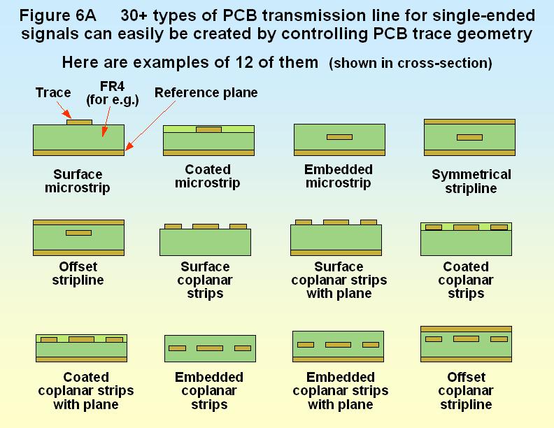
A matched transmission line is a conductor that maintains a fixed ‘characteristic impedance’ – which we call Z0 – from its source to its load, and then its source and/or load ends are terminated (matched) in a resistance having a numerical value equal to Z0. More than thirty different types of transmission line can easily be created on a PCB simply by controlling trace geometry, and some of them are shown in Figure 6A.
PCB transmission lines can easily be extended off a PCB, or between PCBs, using ‘controlled-impedance’ connectors and cables. Controlled-impedance connectors and cables are available as standard products with 50Ω, 75Ω, 100Ω and other characteristic impedances. Most of us are very familiar with 50Ω or 75Ω BNC and their associated 50Ω or 75Ωcables, or with the 100Ω unshielded twisted-pair cables used by numerous low-cost serial data busses.
Transmission line techniques can be used in PCB design to achieve signal integrity (SI) so that the assembled board functions correctly. They can also be used to improve the EMC of a PCB, helping to reduce products’ costs of manufacture.
Cost of product manufacture is reduced because improving a PCB’s EMC performance reduces the specifications for shielding and filtering at the next higher level of assembly – where the cost of achieving the same EMC performance is typically 10 times higher. The financial and commercial benefits associated with achieving good EMC performance from the PCB itself were discussed in some detail in [6] and will not be repeated here.
There is a very great deal of information on using transmission line techniques in PCBs available in textbooks, articles, papers and presentations – but most of it concerns signal integrity (SI), not EMC. Also, most of the computer-aided tools for helping with transmission line design are also concerned with SI and not EMC.
However, all this SI information is helpful for EMC because high-speed or high-frequency SI issues are simply a subset of EMC, for the reasons described in [7]. Designing a PCB for good EMC automatically achieves excellent SI, so we can turn this around and use SI design techniques and tools but set much tougher SI specifications. For example: if we could accept a signal overshoot of (say) 30% for SI reasons, we would achieve better EMC at the level of the PCB assembly by ensuring that the maximum overshoot is, say 10%. Less than 10% overshoot would give even better EMC, but below 3% it becomes hard to say whether a lower specification would be worthwhile.
The only high-frequency SI issue that might not always correlate with good EMC design is crosstalk between traces and devices in the same area of a PCB. However, the segregation techniques described in [8] will reduce crosstalk between different areas (zones) of a PCB and thus contribute to SI.
Some of the design techniques described in this article (e.g. on changing PCB layers) can be used to improve the EMC of any traces, even those that are not matched transmission lines.
There is a great deal of mathematics and theory associated with transmission-line design, and designing transmission lines often runs up against real-world constraints so that the resulting design may not be ideal for SI. SI issues (including crosstalk) are not discussed in any detail here, as they are very adequately covered in a number of good textbooks and relevant standards (see the lists at the end, and [12]).
The usual discussion of EMC aspects of transmission lines focuses on their emissions, but it is important to understand that anything that allows some of the wanted signal to escape as electromagnetic emissions represents an ‘accidental antenna’ – and these antennas will also pick up electromagnetic fields in their environment and convert them into noise signals in their circuits, causing immunity problems. The ‘principle of reciprocity’ is usually invoked here – but without going into theory we can simply note that any circuit that has excessive emissions at frequencies related to its wanted signals will also tend to be susceptible to external electromagnetic fields at those frequencies. So, by reducing emissions by careful PCB layout, we also improve immunity and reduce the amount of space and cost required by filtering and shielding.
1.2 Propagation velocity, V and characteristic impedance, Z0
The dielectric constant of (εR) of the glass-fibre FR4 material used in typical PCBs is around 4.2 at frequencies between 1MHz and 1GHz. Another common glass-fibre PCB material is G-10, which has anεR of about 5.0. This article will focus on FR4, but apart from the differences in εR it applies equally well to G-10 and similar materials. The ceramic material used in some hybrid circuit devices and PCBs has a εR of about 10, and most homogenous plastics and resins have an εR between 2 and 3.
Every conductor in the real world has inductance L and capacitance C per unit length. These parameters depend on the conductor’s shape and its geometry with respect to the conductor(s) carrying its return current. They also depend on the relative permeability µR and the εR of the materials associated with the conductor (in the case of a typical PCB trace: copper, tin/lead alloy, FR4, solder resist and air) and on its proximity of other conductors and insulators. In PCB design the expression εr is usually replaced with k – so that is what will be used in the rest of this article when referring to PCB substrate materials.
The L and C per unit length of a conductor have two effects on the electrical signals and noises it carries –
- they control their velocity of propagation (V): V = 1/√ (LC)
- and they determine their characteristic impedance (Z0) – the ratio of the voltage to the current in the conductor: Z0 = √ (L/C)
It is important to remember that the L and C parameters above are ‘per unit length’, and that the unit length employed must be very much smaller than the wavelength (λ) at the highest frequency of concern for EMC. It is usually more meaningful for digital design to say instead that the unit length employed in analysing V and Z0 must be very much smaller than Vπtr, where tr is the actual rise time of the signal (use the actual fall time tf instead if it is shorter).
Normal PCB traces have L and C values that vary from section to section along their length, and even within a section. Consequently their V and Z0 vary along the length of the trace. Variations in V can cause skew problems, and increase emissions from differential signals (see later). Traces used as transmission lines must maintain a fixed value of Z0 from their start to their finish, and more than thirty different types of transmission line can easily be created on a PCB simply by controlling trace geometry (see Figure 6A).
All discrete components have inductance and capacitance, and when these are connected to a trace they alter its V and Z0 at that point. So circuit details are also important when designing matched transmission lines.
1.3 The effects of impedance discontinuities
Changes in Z0 and errors in the line matching resistors reflect the leading and trailing edges of digital signals or transient noises, and they also reflect RF sinewave analogue signals and noises. The greater the impedance error – the greater the percentage of the signal reflected. We can calculate the ‘coefficient of reflection’ at an impedance error as: (Z1 – Z0)/(Z1+ Z0), where Z1 is the characteristic impedance of the discontinuity.
Reflection coefficients can take any value between +1 and –1. When Z1 is larger than Z0 the reflection coefficient has a positive value, which means that the reflected proportion of the signal adds to the original signal level, on that part of the line. So a voltage step of 2V hitting an impedance discontinuity with a reflection coefficient of +0.5 would result in a step-up to 3V passing backwards along the signal’s previous path.
When Z1 is smaller than Z0 the reflection coefficient has a negative value, which means that the reflected proportion of the signal subtracts from the original signal level, on that part of the line. So a voltage step of 2V hitting an impedance discontinuity with a reflection coefficient of -0.5 would result in a step-down to 1V passing backwards along the signal’s previous path.
In the case of the line terminating resistors, we replace Z1 in the above equation with ZS, the impedance at the signal’s source to find the for reflection coefficient at the trace’s driven end. And for the other end of the trace (receiver) we replace Z1 with ZL, the impedance of the load (receiver) to find the reflection coefficient at the trace’s load end.
When a PCB trace is not intentionally designed as a matched transmission line, reflections can occur at many places: at either or both of its ends, and along its length. Reflected signals and noises will flash backwards and forwards along the trace (or parts of it) many times before eventually subsiding to a steady state. This effect is easily seen with a very fast oscilloscope, or with a very long trace. Figure 6B shows two examples where a trace has a constant characteristic impedance along its length, but is not correctly terminated with matched values of resistors at either of its ends.
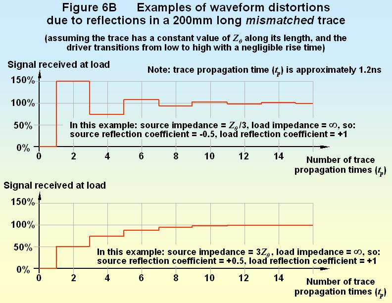
Waveforms like the upper one in Figure 6B are obviously capable of crossing a logic threshold twice, which can lead to the misbehaviour of digital circuits. Avoiding this is one of the key goals of SI design.
Notice that Figure 6B shows the waveforms experienced at the ends of the trace. Different waveforms will be experienced by devices positioned along the trace, between its two ends. The ‘rules’ used to draw Figure 6B are given in [13] and the various textbooks, standards and other references listed at the end, and they can also be adapted to determine the waveforms at any point along a trace.
Reflections make mismatched conductors act as ‘accidental antennas’ and emit a proportion of their reflected signals into the air as radiated emissions, which is bad for EMC. If the distance between a pair of impedance discontinuities happens to be the same (or near to) a quarter or half of the wavelength of a significant spectral component of the signal or noise – that part of the conductor will resonate, making it a much more efficient accidental antenna, as shown by Figures 6C and 6D. Whether the resonances occur at quarter or half wavelengths depends on the type of the discontinuities at each end.
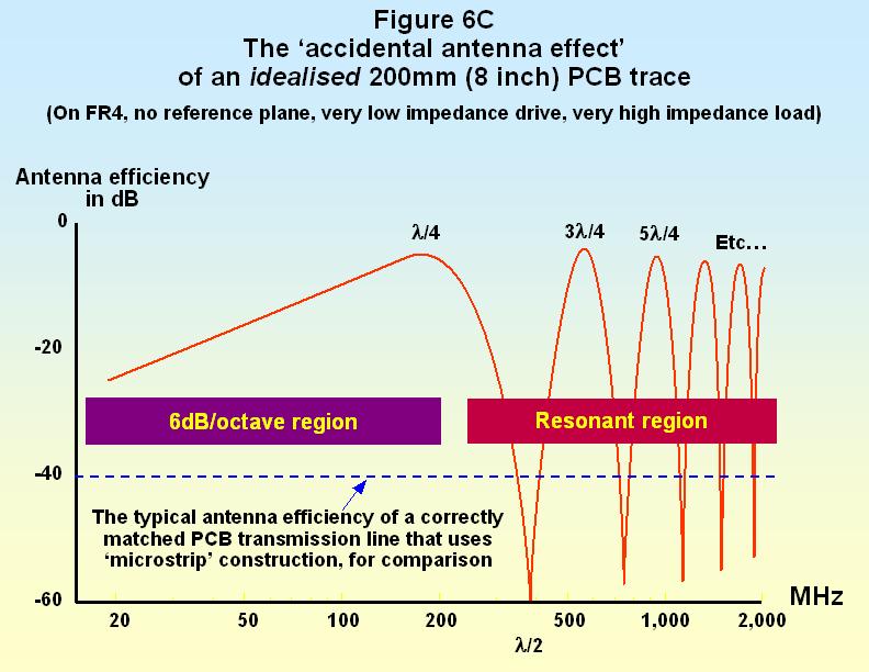
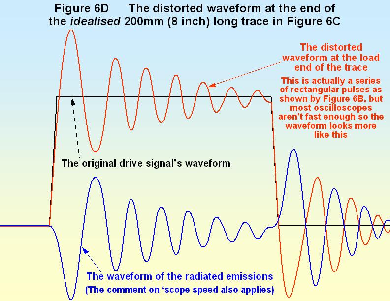
The accidental antenna efficiency of a real trace, and the real-life drive and load waveforms, will not be exactly the same as the idealised sketches in Figures 6C and 6D. These sketches are simply trying to communicate how ignoring matched transmission line design can lead to excessive emissions. However, it is surprising how many clock waveforms end up looking very much like the red curve in Figure 6D.
When traces act as accidental antennas, this is not only bad because of their unwanted emissions, it is also bad for immunity because they are more effective at picking up electromagnetic fields from their environment and converting them into conducted noises in the traces.
1.4 The effects of keeping Z0 constant
Keeping Z0 constant along a conductor from the source to the load, and terminating the ends of the conductor in matched resistances, prevents reflections and communicates almost 100% of the signal. This is very good for SI and also very good for EMC. As was said above, many modern products that employ digital processing and/or wireless technologies could not even work without matched transmission lines, much less meet their EMC requirements for reliability and compliance.
Where a signal needs to pass from one transmission line to another with a different characteristic impedance, this may be achieved by the use of an impedance-matching transformer which does not cause a significant impedance discontinuity. The frequency response of such transformers can cover three decades but cannot extend down to d.c., so they are not suitable for all applications.
1.5 Time Domain Reflectometry (TDR)
The PCB structure and its trace routing is becoming a great problem for impedance matching as digital signal or noise rise and fall times decrease below about 150ps, or as analogue signals or noise increase above 2GHz. For such signals or noises PCB trace routing structures that used to be able to be ignored, such as via holes, now need to be treated as impedance discontinuities along a transmission line [9].
An important tool for simulating and visualising this problem, and for measuring real PCBs to discover if they have been designed correctly or to trace errors, is Time Domain Reflectometry (TDR). Signals are input to a simulated or real PCB structure and the timing and amplitude of the reflections simulated or measured, and the results analysed and displayed as a graph of impedance versus time [10] [11]. The usefulness of the TDR graphs is that they show the designer where, along a trace, an impedance problem is occurring and how serious the problem is. Figure 6E shows an example of a TDR measurement made with three different rise/fall times, and was developed from Fig 4 of [9].

Figure 6E shows how digital signals with rising and falling edges of 1ns see the averaged impedance of a PCB trace. The effects of connectors and via holes on the characteristic impedance are ‘smoothed out’ by the slow rise and fall times. But as a signal’s rise/fall times reduce the effects of the impedance discontinuities due to connectors, via holes and other details become more apparent, as shown by the TDR curves for rise/fall times of 300ps and 150ps.
Serial data at 2.5Gb/s uses non-return-to-zero (NRZ) coding to employ a fundamental frequency of 1.25GHz, implying a maximum rise (and fall) time of under 200ps to achieve a reasonably open ‘eye pattern’. Since the intention is to increase the serial data rate to 5 and 10GHz in the next few years, we clearly need to be concerned about maintaining transmission line matching with rise and fall times of 150ps or less – so connectors and via holes are going to present significant problems. Techniques for dealing with some of the issues are discussed below.
In the 150ps curve of Figure 6E the TDR feature corresponding to the location of impedance matched connector shows that its impedance is around 60Ω, and the rounded top of its curve suggests that this impedance would not change much if signals with even shorter rise/fall times were employed instead. 60Ω is not a perfect match for the 50Ω transmission line, and creates a reflection coefficient of +0.09, but it is much better than the connector that connects the signal cable to the PCB.
But the TDR feature that corresponds to a via hole is still quite sharp even with the 150ps rise/fall time signal. A via hole is too short for this signal to show any flattening or rounding off of the curve that which would imply that its actual impedance was no longer being ‘smoothed out’ by the risetime. So in the case of the via hole we should expect that signals with rise/fall times shorter than 150ps would experience even lower impedances, higher reflection coefficients and worsened SI and EMC.
1.6 When to use matched transmission lines
The crude guide for SI is to use matched transmission lines when the propagation time (tp) along the entire trace from the source to the final load equals or exceeds half of the signal’s real rise time: tp ≥ tr /2. If the real fall time (tf) of a signal is shorter than its real tr, the value for tf should be used instead.
When tp≥tr /2 it is usually considered that transmission line techniques are required so that waveform distortion and eye-pattern closure will be acceptable for SI. But some engineers are a little more careful and prefer to use transmission line techniques for SI when tp exceeds tr/3, or even less.
The aim of these crude guides is to ensure that the first reflection due to a mismatched trace occurs during the rise (or fall) time of the signal, where it will (hopefully) be masked by the rising edge and cause no problems for the receiver. If the trace was so long that its first reflection occurred after a logic transition had finished, the result could easily be double clocking or other digital glitches, so it becomes necessary to use matched transmission line techniques. Significant overshoot and ringing could still occur and so these guides might not be good enough for SI for some devices, and they do not control EMC as well as is often required for greatest cost-effectiveness in product design. Always read all the application notes for a device carefully to see if it has more stringent requirements than the above guides.
If the length of a trace is lt and the velocity of propagation along the trace is V, then that trace’s tp is given by: tp = lt /V. So we can modify the above guidance to say that: for SI, transmission line techniques are necessary when lt ≥ V.tr /2 or less.
For example, a stripline in an FR4 PCB with k = 4.2 has a bare-board V of 6.8ps/mm (see a later section), so a digital signal with a rise/fall time of 2ns (actual values, not data sheet specifications, see later) would need to use matched transmission lines for any traces that are longer than 147mm, for acceptable SI (98mm for the ‘more careful approach).
We all like to use simple arithmetic to save time, but it is important to be aware that the above guides really are very crude indeed. Their assumptions about logic thresholds, eye patterns and EMC may not be true for other types of devices. And they take no account of the effects on V and Z0 of the capacitive loading of vias and devices (see later) or of the return path inductance caused by via holes or imperfect planes (also see later).
Engineers who take account of these complicating issues can achieve good designs in less time than those that merely follow the crude guides above. In fact, for good SI, a final design might require the use of transmission line techniques when tp exceeds a value that lies between tr/3 and tr/10.
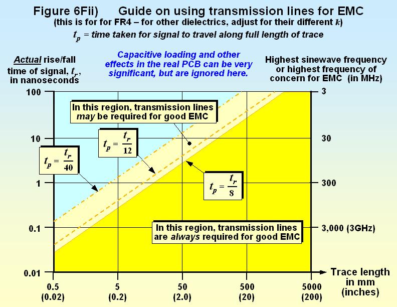
Figure 6Fi) shows these various guides on a graph of rise/fall time against trace length.

From Figure 6C we can see that when a plain trace on a bare FR4 PCB has a length of about one-fortieth of the wavelength at the highest frequency of concern, it has an ‘accidental antenna efficiency’ of about –20dB. To prevent traces becoming more efficient antennas than this, the equivalent of the crude tp ≥ tr /2 guide is that we should use tp ≥ tr /8 to determine how long a trace can be before we need to use matched transmission line techniques for good EMC. In frequency terms (see a later section) we can write this instead as tp ≥ 1/8πf, where f is the highest frequency of concern.
Of course, using transmission line techniques for even shorter traces should improve EMC even more. The EMC equivalent of the ‘more careful’ approach is to use transmission line techniques when tp exceeds tr /12. Continuing the example used above for SI, for good EMC a matched transmission line should be used where the trace length exceeds 37mm (or 25mm when using the ‘more careful’ approach).
But the above EMC guides are based on crude assumptions, and it may even be that good EMC requires the use of matched transmission lines when tp exceeds a value that lies between tr /12 and tr /40.
Figure 6Fii) shows these various guides on a graph of rise/fall time against trace length.
To avoid the uncertainties in the above guides, simulation techniques are recommended. For good SI these should simulate the final design (the full details of the final PCB layout, plus all of its device loads) for all traces for which the bare-board tp ≥ tr/10, or tp ≥ 1/10πf.
For good EMC the final design should be simulated – at least for all traces carrying ‘aggressive’ or ‘sensitive’ signals (see later) – for which the bare-board tp ≥ tr/40, or tp ≥ 1/40πf (f being the highest frequency of concern).
Simulation is becoming increasingly affordable – and increasingly necessary in modern PCB layouts (a section on simulation is included later in this article). Where simulation is not an option, but good line matching is nevertheless required, the references given later provide some simple formulas that allow the effects of vias, stubs, load capacitance and imperfect return current paths to be taken into account. These calculations are not as accurate as simulation, so add an ‘engineering margin’ of at least 25% to their results.
1.7 Increasing importance of matched transmission lines for modern products
Some modern high-speed interconnections can launch two or more data bits before the first edge of the first bit has even reached the end of the trace. Reflections at impedance discontinuities along the trace and at mismatches at its ends cause data-pattern-related noise on the line – as well as overshoot and ringing on rising and falling edges. The increasingly short real rise/fall times of modern sub-micron ICs are less tolerant of PCB layout, as Figure 6E shows.
So it is becoming more important to more accurately match and maintain Z0 along the whole length of a transmission line. Even via holes are becoming significant. Microwave design techniques (e.g. adding ‘stubs’ of certain lengths) are increasingly needed to maintain Z0 within close tolerances for every millimetre along a trace.
1.8 It is the real rise/fall times that matter
When designing a PCB, the focus is naturally on the traces carrying signals with high edge-rates or the high frequencies, but even signals with a low frequency can cause excessive emissions. For example, a 1kHz clock generator with extremely short rise and fall times has caused emissions test failure all the way up to 1GHz; and a pulse-width-modulated (PWM) drive for a brushless DC motor has interfered with 6GHz radio communications, despite the switching rate being just a few tens of kHz.
Data sheet rise/fall time specifications (where they exist at all) are almost always just the maximum for the temperature range concerned – but actual rise/fall times are (almost) always shorter than data sheet specs, often a half or a quarter of the specified maximum.
In addition, older devices may have gone through a die-shrink or two, to put them on smaller silicon processes that make more money for their manufacturers – if so, their rise/fall times will be very much less than their data sheet specifications. Examples include HCMOS and ‘F’ series TTL ‘glue logic’ devices, the data sheets for which still quote the same rise/fall times as they did in 1985. But the actual silicon features used in current distributor stock of these IC types could now be ten times smaller than in 1985, and their rise/fall times could be at least ten times shorter than the maximum figures in their data sheets. HCMOS ICs are specified as having rise and fall times no longer than 5ns – but experience at the time of writing shows they can cause significant emissions at up to 900MHz, implying that their real rise/fall times might be as low as 300ps.
Another issue, mentioned briefly above and covered in more depth later, is that the capacitive loading of a trace, for example by connecting a number of devices along its length, reduces V even further. So it could very easily be the case that a well-established type of IC with data sheet rise/fall times of 2ns (e.g. ‘F’ series TTL) – driving a multidrop bus – may need to use matched transmission lines for SI when trace length exceeds 20mm.
It is vital to know the actual rise/fall times of the digital signals that will be used in a PCB. It is impossible to do transmission line design using data sheet specifications for the vast majority of ICs. But few manufacturers even seem to know the rise/fall times of the devices they are currently manufacturing (and they care even less). To try to encourage manufacturers to supply this essential design data, we should all make sure we always ask for real rise/falltime data, including their maximum and minimum values (see “Ask For It” in [12]).
Given the lack of hard data on rise/falltimes it is often necessary to use a high-speed oscilloscope with high-frequency probes and probing techniques (the ‘scope manufacturer will advise) to measure real circuits. An oscilloscope/probe combination with a bandwidth of BW has a rise/fall time of about 1/(πBW) (BW in GHz gives rise/fall time in ns). So a BW of 1GHz would imply that a ‘scope/probe combination has a rise/fall time of 320ps – making it difficult to accurately measure signals of less than 1ns. With such a scope, if a digital signal was measured as having a rise time of 330ps, the actual rise time of the signal could be anywhere between 10 and 200ps. To measure rise times of 100ps typical of PCI Express needs an oscilloscope/probe combination with a BW of around 7GHz – not a trivial requirement.
Luckily, there are an increasing number of ICs that are designed with slew-rate-controlled driver outputs. These have been produced to make it easier to send fast data over transmission lines, and sometimes to improve EMC as well. Such ICs are always to be preferred over the more usual type that switches as fast as its silicon processing allows, whether the user needs such short rise/fall times or not. There is more discussion of drivers later.
In some industries it is normal for design to be progressing on the basis of an IC that is not yet available for testing. Where these are ASICS or FPGAs, and if data on real rise/fall time is not available (even from IBIS or SPICE models) it may be possible to obtain another type of IC made using the same types of drivers, and measure their rise/fall times in a test board. Where it is impossible to obtain a good estimate of the real rise/fall time data for an IC that will be using a sub-micron silicon process, it is often best to lay the PCB out with filters on all the driver outputs that could toggle at more than 1kHz, but only fit the filter components if SI or EMC tests show they are necessary. Filtering is covered later.
If the ICs used will always have rise/fall times of at least 1ns (despite possible die-shrinks in the future) or else are filtered (see later) to achieve the rise/fall times – transmission line design is not very difficult, and much of this article will be redundant.
1.9 Noises and immunity should also be taken into account
Designers usually only consider using transmission line techniques for signals that have high data rates or high sinewave frequencies, but as was mentioned above it is the rise/fall times that matter for digital signals – not their clock or data rate. But reducing the emissions caused by unwanted noises, and/or improving immunity, can also be good EMC reasons for using transmission lines.
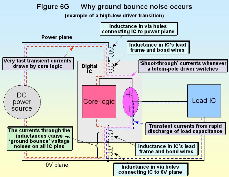
Digital ICs suffer from ‘ground bounce’ noise, and its equivalent ‘rail bounce’ noise (sometimes called rail collapse noise). A large part of this noise is what is known as simultaneous switching noise (SSN) or simultaneous switching output (SSO). Whenever an output pin changes state, the current it draws from its ICs 0V and power rails eventually flows through the interconnections to the PCB’s 0V and power rails. The inductance in these paths causes voltage drops that make the IC’s internal 0V and power rails ‘bounce’ with respect to the PCB rails, according to the activity of the output ports. This process is shown by Figure 6G for ground bounce, but rail bounce is caused in the same way.
This means that the logic high and low levels from a device’s output pin, that we often assume to be static levels, can be very noisy due to the operations of the other outputs on an IC. Some device manufacturers include SSN/SSO specifications on their data sheets – obtained by measuring one static output whilst all of the other outputs are toggled at a specified rate when driving specified load impedances. For SI reasons it is important that SSN/SSO noise is less than the logic threshold of the device the static output is connected to, but this is not always achieved – sometimes it is necessary for reliability reasons to alter a product’s software to reduce the number of outputs on a device that can change state at once.
The ‘core logic’ processing in digital ICs is not connected directly to any output pins, but its operation modulates the power supply current drawn by an IC and so adds to the ground and power bounce noise. The core logic of some Xilinx FPGAs (and probably those of many other manufacturer’s ICs too) can have power current demands with 50ps durations – equivalent to a noise frequency spectrum that extends to at least 13GHz.
All this means that even ‘static’ digital signals can be very polluted by very high frequency noise. When this noise travels on traces that are not properly matched transmission lines, their ‘accidental antenna’ effects can make them a source of emissions. So it may be necessary to either filter out this noise (see later) or else treat the lines as matched transmission lines to reduce their accidental antenna efficiency.

Immunity is also a topic hardly ever discussed in connection with transmission lines. But reducing a trace’s ‘accidental antenna efficiency’ by making it a matched transmission line (especially a stripline) can be a big help in improving the immunity of any signals, analogue or digital.
For instance, a reset line on a PCB is considered to be a static line, only changing state very occasionally. But it can be a long trace and hence a very effective ‘accidental antenna’ (if not treated as a transmission line) and so it can be a significant emitter of the very high frequency ground-bounce noise created inside the ICs it is connected to. Its long length and good accidental antenna characteristics also make it an easy route for interference to get into an IC and cause it to misoperate or even be damaged. A later section goes into these topics in more detail.
Filtering ‘static’ traces at each IC they are connected to easily prevents these EMC problems (see later). But filtering may not be a viable solution for all of the non-transmission line traces on a PCB, so it may prove necessary to treat them as transmission lines just to reduce their efficiencies as accidental antennas.
1.10 Calculating the waveforms at each end of a trace
Knowing the source impedance of a driver chip when pulling up or down (they are different), plus the characteristic impedance and tp of a trace designed as a transmission line, and its load impedance, makes it easy to hand-calculate the waveforms and timing at the driving and receiving ends of the trace (and any point in-between). The “Lattice Diagram” is a graphical method of keeping track of these calculations and what they represent.
This process is complicated by the fact that actual driver output impedances vary according to the voltage and current they are outputting, and whether they are pulling up or down. “Bergeron Plots” using device manufacturers’ data make it easy to discover what their actual impedances are. Sometimes they can have higher impedances than the Z0 of the traces they drive, so their actual output voltage is severely attenuated at first.
Rather than describe the above process in this article, the author instead refers the reader to the excellent Motorola (now called Freescale) application note AN1051 [13]. This document assumes that the characteristic impedance is constant along a trace, but as Figure 6E shows this may not be a safe assumption when real rise/fall times are under 1ns, as many now are unless they have been filtered to slow them down.
A small mismatch along a line, or in its resistive terminations, might make very little difference to the voltage waveform. But mismatches of under ±10%, that are often perfectly acceptable for SI reasons, can cause large overshoots in the trace’s current waveform, significantly increasing emissions from the PCB.
1.11 Examples of two common types of transmission lines
Figure 6J shows an example of a commonplace type of PCB transmission line – the symmetrical stripline – which is a trace on an inner layer of a PCB that is spaced half-way between two reference planes. The reference planes are assumed to extend a great distance on all sides of the trace, and beyond its ends. A simple formula that provides an estimate of its characteristic impedance Z0 in Ω is:
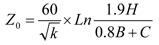
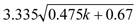
– where k is the dielectric constant of the PCB’s substrate (typically 4.2 for FR4 above 1MHz); B is the trace width; C is the thickness of the copper material used; and H is the substrate thickness. Note that it does not matter which length units are used in this equation: millimetres, inches, miles or whatever – as long as they are consistent, the answer is in ohms.
The propagation velocity V for a stripline in ns/metre (or ps/mm) is:
 (approx. 6.83ns/m or 6.83ps/mm for FR4).
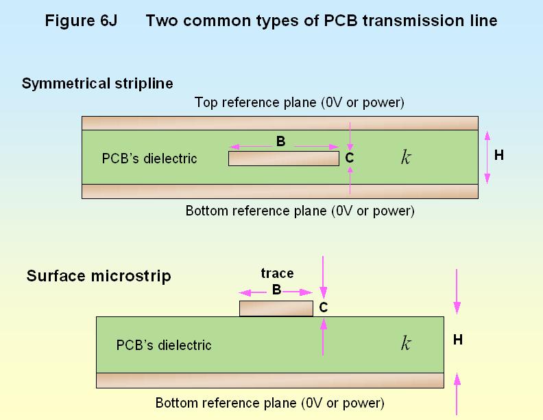
Figure 6J also shows the second example of a commonplace type of transmission line – the surface microstrip. This consists of a trace on an outer layer of a PCB over a large reference plane (on an inner layer of the PCB). The reference plane is assumed to extend a great distance on all sides of the trace, and beyond its ends. A simple formula that provides a guide to its characteristic impedance Z0 in Ω is:

The propagation velocity V for a microstrip in ns/metre (or ps/mm) is:
 (approx. 5.5ns/m or 5.5ps/mm for FR4).
V in microstrip is a little faster than V in a stripline, because in a stripline all of the electric field lines around the trace travel in the dielectric, so its C0 is higher than in a microstrip, where some of the electric field lines travel in the air outside the PCB. But the electric field lines in the air mean that microstrip is a bit ‘leakier’ than stripline, so when we consider emissions we always prefer striplines for good EMC.
Formulae for calculating Z0 of a large number of types of PCB transmission line geometries are given in the standards IEC 61188-1-2:1998 from http://www.iec.ch/webstore, IPC-2141 and IPC-2251 from http://www.ipc.org. IPC-2251 replaces IPC-D-317A. These standards also include a great deal more useful information on designing with PCB transmission lines.
But it is now easier, and more accurate to use computer-aided design tools to calculate Z0 and other aspects of transmission lines. The types of tools available include numerical solvers and field solvers. They provide much more accurate analysis, are now easy to use, and allow quick ‘what if’ assessments. A number of free transmission line calculators can be downloaded from the Internet (see the references at the end), but better ones can be purchased, for example from companies that provide CAD packages for PCB design.
Many of the available tools assume ideal transmission lines (e.g. with infinite reference planes), but some are real field solvers, and some can now deal with real, complex PCBs including capacitive loading – see the section on field solvers below.
1.12 Coplanar transmission lines
These can be useful when a transmission line needs to be routed without a reference plane on an adjacent layer. Routing signal traces run side-by-side with return (0V) traces is a good EMC practice, even when not using transmission lines, but for a coplanar line over a plane the 0V traces should be via’d to an unbroken (solid) 0V plane every λ/10 (or less) at the highest frequency of concern.
1.13 The effects of capacitive loading
It was mentioned above that capacitive loading on a transmission line reduces the velocity of propagation of signals along it (V) and also reduces its characteristic impedance (Z0). Many transmission line equations, calculators, articles, papers and textbooks assume ideal PCBs, with no via holes, connectors or ICs. Their omissions are a common cause of additional PCB design iterations – some traces may need to be treated as transmission lines, when the bare-board calculations had shown they would not; some traces may need their geometry or termination resistors modifying to achieve better matching. To improve time-to-market we must design real-life transmission lines, which means taking capacitive loading into account.
One cause of capacitive loading is the pins of the ICs or other devices (diodes, transistors, etc.) connected to a transmission line. There is always such a device at each end of a trace, where their capacitance will have some effect on the quality of the line termination but will not alter the line’s Z0 or V. It is the pins of devices that are connected along a line, such as a typical multidrop bus (e.g. microprocessor memory and address busses) that will reduce the line’s Z0 and V.
We must not overlook the effects of stray capacitances either. There is a stray capacitance at every via hole (typically in the range 0.2 - 2pF) causing a local reduction in impedance (see Figure 6E). A transmission line trace with a lot of vias in it will have lower than expected average Z0 and V. More detail on via capacitance is given in “Via Capacitance” and other articles in [12].
“Resonances in Short Transmission Lines” in [12] describes how capacitive loading at the end of a line can cause huge amounts of ringing and overshoot in traces that would be ignored when following the crude guides given earlier.
If a metal object such as a heatsink or a sheet of metal such as the wall of an enclosure is placed close to a microstrip transmission line it will also add stray capacitance to the trace. Plastic objects or sheets, cables or condensation close to a microstrip line will also increase its stray capacitance. The only thing that should be within 5mm of a microstrip line is air or a similar gas, or vacuum.
The reference planes on both sides of a stripline shield it from the stray capacitance of nearby metal or plastic, but it is still affected by the capacitance of device pins that connect along its length.
In some cases, the effects of capacitive loading can be compensated by reducing the width of the trace in the effected region, and “Potholes” in [12] provides some calculations appropriate for ‘point’ capacitances such as vias or device connections.
It may be practical to use a technique used by microwave RF designers – adjusting the diameters of vias and their pads and the clearance holes (‘antipads’) in the planes they penetrate, to maintain the desired value of Z0 through the via holes. But some RF design techniques are bad for EMC in general – in this case making large holes in reference planes can cause problems for return currents. They can also increase plane impedance, leading to higher levels of CM emissions and poorer immunity.
Simple formulae for the effects of capacitive line loading are given in [13], as follows:
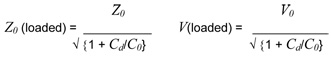
where: Cd is the load capacitance per unit length
C0 is the intrinsic (bare-board) line capacitance per unit length
V0 is the intrinsic (bare-board) line velocity
Cd is easy to calculate from a PCB’s circuit design. For example: if a 150mm long section of trace is connected to one pin each on ten ICs, and the capacitance for each via hole, pad and IC pin totals 10pF, then we have 100pF spread along 150mm of trace, making Cd equal to 100/150 or 0.667pF/mm (667pF/m).
C0 and V0 can be found from formulae given in IEC 61188-1-2:1998. Where a line’s V0 and Z0 are already known, its C0 can be found from: C0 = √k/(V0xZ0). So, for C0 in pF/mm: C0 = √k/(0.3xZ0).
But it will generally be better and more accurate to extract C0 and V0 from draft PCB layouts, using a field solver (see later), for each individual section of a trace.
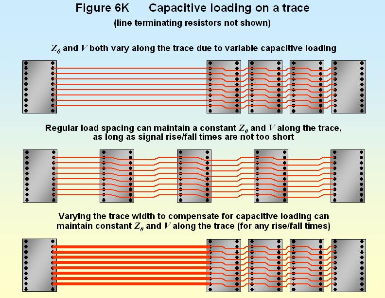
The length of trace to which the above expressions should be applied depends on the rise/fall times (or highest frequencies of concern) of the signals or noises to be controlled. Where the rise/fall time is so long that the whole length of a trace and its capacitive loads (due to IC pins, via holes, or other physical features) can be treated as one average value, the above expressions can be applied to the whole trace. (For example, see the 1ns curve on Figure 6E.)
But where the rise/fall time is short enough for significant impedance discontinuities to arise within the length of a trace (for example, see the 300ps curve of Figure 6E) the above expressions can be used over trace sections short enough to be treated as an average impedance value. The trace width can then be varied within each section, depending upon the capacitive loading of that section, so that every section has the same impedance.
But where rise/fall times are very short (or frequencies very high), even features as short as 1mm may create unacceptable impedance discontinuities (see the 150ps curve on Figure 6E.) and the above expressions may no longer be useful. If these signals or noises cannot be low-pass filtered, the only solution may be to design the circuit differently, for instance by using point-to-point serial data busses instead of multidrop parallel ones (circuit design is discussed in a later section). A useful technique is to route the trace on a single layer, so that it has no via holes along its length.
Because the rise/fall times of digital devices based on modern silicon processes are naturally so small, and getting smaller [6] – and because the frequencies of the ‘core noise’ that leaks into their I/O pins are naturally so high, and getting higher [6] – the problems of trying to create transmission lines that are well matched along their entire lengths are getting much harder, unless the signals can be low-pass filtered (see later).
1.14 The need for PCB test traces
Process quality variations in PCB bare-board manufacturers can cause out-of-specification batches of assembled boards to be made. It is very important that such boards do not have value added to them (by assembly) before their dire nature is exposed. So it can be important to include ‘test traces’ (sometimes called ‘test coupons’) on the PCB, so that PCB batches can be checked for Z0 and V upon delivery, before they are accepted into the company’s stores.
Appropriate test instruments, suitable for use by non-specialists in a production environment, are required for testing the coupons, and one manufacturer of such instruments is Polar Instruments [14]). The design of the test coupons so that a PCB can be fully characterised at Goods Receiving is covered by [15].
An example of a process issue is variations in trace width, caused by under- or over-etching. In a modern PCB manufacturing plant, the variations from batch to batch are usually less than 13 microns (0.5 thou) and the effect of this on Z0 is usually only considered to be significant when trace widths are less than 0.13 mm (5 thou). But differential lines are very sensitive to this problem (discussed in detail later).
1.15 The relationship between rise time and frequency
Digital hardware engineers work in the time domain, and for them a digital signal is a different voltage level bracketed by rising and falling edges. But EMC and RF engineers work in the frequency domain, using spectrum analysis tools. For them, a digital signal is a ‘comb’ of harmonics starting at the fundamental frequency: the data rate. When trying to design PCBs for good EMC, it often helps to be able to relate the time domain to the frequency domain, and vice-versa. Doing this properly requires Fourier transforms, and some digital oscilloscopes are fitted with Fourier post-processing options allowing a captured waveform to be viewed in the frequency domain. The author is not aware of any spectrum analysers that offer inverse Fourier transforms, converting measured spectra into waveforms.
The spectrum of the harmonics of a digital signal continues to infinity, but the frequency (f) at which its harmonics start to diminish rapidly and very soon become negligible is given by: f = 1/πtr. (This relationship can be seen in the two vertical axes of Figure 6F, the real rise time on the left and the equivalent ‘highest frequency of concern’ on the right.) So a signal with 1ns rise and fall times when viewed on a spectrum analyser or EMC receiver has a ‘comb’ of harmonics that have significant amplitudes to at least 318MHz.
The guidance given earlier said that, for good EMC, accurately matched transmission line techniques are strongly recommended when lt ≥ V.tr /8, although a more careful approach would use them whenever lt ≥ V.tr /12, or less). Simulation of the final design (including device loading) is recommended when lt ≥ V.tr /40.
Now we can convert this into guidance for sinewave signals or noises: accurately matched transmission line techniques are strongly recommended when lt ≥ V /8πf, although a more careful approach would use them whenever lt ≥ V / 12πf). Simulation of the final design is recommended when lt ≥ V /40πf.
The broadband sinewave signal designer’s equivalent of overshoot and ringing is the flatness of the amplitude versus frequency response, whereas for a narrowband (fixed frequency) sinewave designer it is just a matter of gain. Using the SI guides above could result in several dB of ‘flatness’ variation, or a few dB gain error. Using matched transmission line techniques for traces longer than V /12πf, or even shorter traces, may be required where amplitude flatness or gain specifications are tight.
Hopefully, this section will allow readers who prefer to work in the frequency domain to quickly convert from the frequency to the time domain (e.g. from millimetres to GHz), and vice-versa.
12 References
[1] “Design Techniques for EMC” (in six parts), Keith Armstrong, UK EMC Journal, Jan – Dec 1999
[2] “Design Techniques for EMC” (in six parts), Keith Armstrong, http://www.compliance-club.com/keith_armstrong.asp
[3] “PCB Design Techniques for Lowest-Cost EMC Compliance: Part 1”, M K Armstrong, IEE Electronics and Communication Engineering Journal, Vol. 11 No. 4 August 1999, pages 185-194
[4] “PCB Design Techniques for Lowest-Cost EMC Compliance: Part 2”, M K Armstrong, IEE Electronics and Communication Engineering Journal, Vol. 11 No. 5 October 1999, pages 219-226
[5] “EMC and Electrical Safety Design Manuals”, a set of four volumes edited by Keith Armstrong and published by York EMC Services Ltd., 2002, ISBN 1-902009-07-X, sales@yorkemc.co.uk, phone: +44 (0)1904 434 440.
Volume 1 - What is EMC? ISBN 1-902009-05-3
Volume 2 - EMC Design Techniques - Part 1 ISBN 1-902009-06-1
Volume 3 - EMC Design Techniques - Part 2 ISBN 1-902009-07-X
Volume 4 - Safety of Electrical Equipment ISBN 1-902009-08-8
[6] “Advanced PCB Design and Layout for EMC – Part 1: Saving Time and Cost Overall”, Keith Armstrong, EMC & Compliance Journal, March 2004, pp 31-40, http://www.compliance-club.com/keith_armstrong.asp
[7] “EMC and Signal Integrity”, Keith Armstrong, Compliance Engineering, March/April 1999, http://www.ce-mag.com/archive/1999/marchapril/armstrong.html
[8] “Advanced PCB Design and Layout for EMC – Part 2: Segregation and interface suppression ”, Keith Armstrong, EMC & Compliance Journal, May 2004, pp32-42, http://www.compliance-club.com/keith_armstrong.asp
[9] “Signal Integrity Considerations for High Speed Data Transmission in a Printed Circuit Board System”, Tom Cohen, Gautam Patel and Katie Rothstein, IMAP Symposium 1998, http://www.teradyne.com/prods/tcs/resource_center/whitepapers.html
[10]“Measurements for Signal Integrity”, Vittorio Ricchiuti, 2004 IEEE International EMC Symposium, Santa Clara, August 9-13 2004, ISBN 0-7803-8443-1.
[11]“Gigabit Backplane Design, Simulation and Measurement – the Unabridged Story”, Dr Edward Sayre et al, DesignCon2001, available along with many other relevant papers from: http://www.national.com/appinfo/lvds/archives.html
[12] Howard Johnson’s list of downloadable articles: http://www.sigcon.com/pubsAlpha.htm
[13]“Transmission Line Effects in PCB Applications”, Freescale (previously Motorola) application note AN1051, includes a number of other useful references, go to http://www.freescale.com and search for AN1051 or direct to: http://www.freescale.com/files/microcontrollers/doc/app_note/AN1051.pdf.
Another useful introduction to transmission lines is “System Design Considerations When Using Cypress CMOS Circuits” from Cypress Semiconductor Corporation, Cypress Semiconductor Corporation application note, http://www.cypress.com.
[14]Polar Instruments, http://www.polarinstruments.com/support/cits/cits_index.html
[15]“Printed Circuit Board (PCB) Test Methodology”, Revision 1.6 January 2000, Intel Corporation, www.intel.com/design/chipsets/applnots/29817901.pdf
13 Some useful sources of further information on PCB transmission lines
(These are not referenced in the article.)
John R Barnes, “Robust Electronic Design Reference Book, Volumes I and II”, Kluwer Academic Publishers, 2004, ISBN 1-4020-7739-4 especially chapters 21, 30 and 31.
Hall, Hall and McCall, “High Speed Digital System Design, a Handbook of Interconnect Theory and Practice”, Wiley Interscience, 2000
Howard W Johnson and M Graham, “High Speed Digital Design, a Handbook of Black Magic”, Prentice Hall, 1993, ISBN 0-1339-5724-1
Howard W. Johnson, “High Speed Signal Propagation: Advanced Black Magic”, Prentice Hall, 2003, ISBN 0-1308-4408-X
Mark I. Montrose, “EMC and the Printed Circuit Board, Design, Theory, and Layout Made Simple”, IEEE Press, 1999, ISBN 0-7803-4703-X
Mark I. Montrose, “Printed Circuit Board Design Techniques for EMC Compliance, Second Edition”, IEEE Press, 2000, ISBN 0-7803-5376-5
Brian Young, “Digital Signal Integrity Modeling and Simulation with Interconnects and Packages”, Prentice Hall, 2001
Xilinx ‘Signal Integrity Central’: http://www.xilinx.com, then click: ‘Products & Services’ - ‘Design Resources’ - ‘Signal Integrity’, or go direct to: http://www.xilinx.com/products/design_resources/signal_integrity/index.htm. Also, the Xilinx Xcell on-line journal often carries relevant articles: http://www.xilinx.com/ publications/xcellonline/index.htm.
California Micro Devices: http://www.calmicro.com/applications/app_notes.html or go to: http://www.calmicro.com then click on ‘Applications’ then click on ‘App Notes/Briefs’
Mentor Graphics: http://www.mentor.com, click on ‘Technical Publications’
UltraCAD: http://www.ultracad.com
LVDS: http://www.national.com/appinfo/lvds/
Intel: http://developer.intel.com, or http://www.intel.com/design, or http://appzone.intel.com/literature/index.asp
IBM: http://www-03.ibm.com/chips/products or http://www-3.ibm.com/chips/techlib/techlib.nsf
Note: On the Intel and IBM sites, to find application notes you must first choose a type of device.
Rambus: http://www.rambus.com/developer/developer_home.html
Cypress Semiconductor Corporation, many useful application notes at: http://www.cypress.com
IEEE Transactions (www.ieee.org) on…
– Electromagnetic Compatibility
– Advanced Packaging
– Components, Packaging and Manufacturing Technology
– Microwave Theory and Technology
IEEE (www.ieee.org) Conferences and Symposia on…
– Electromagnetic Compatibility
– Electrical Performance of Electrical Packaging
Printed Circuit Design magazine http://www.pcdandm.com/pcdmag/
CircuiTree magazine: http://www.circuitree.com
IMAP Symposia
DesignCon Symposia
Some free PCB transmission line calculators
http://www.emclab.umr.edu, click on ‘PCB Trace Impedance Calculator’
http://www.amanogawa.com, click on ‘Transmission Lines’, then ‘Java Applets’
http://www.mwoffice.com/products/txline.html
http://www.ultracad.com/calc.htm
Relevant Standards
IEC 61188-1-2 : 1998 from http://www.iec.ch/webstore
IPC-2141 and IPC-2251 from http://www.ipc.org
I would like to reference all of the academic studies that back-up the practical techniques described in this seri